One tungsten diselenide crystal becomes channel, gate oxide and contacts in an IBS transistor
IBS researchers built a transistor out of one tungsten diselenide crystal, switching tenfold in current per 61.3 millivolts. The gate oxide is made from the channel's own top layers, so the design skips the deposition step that has held back 2D electronics.
The Scientist · Science desk
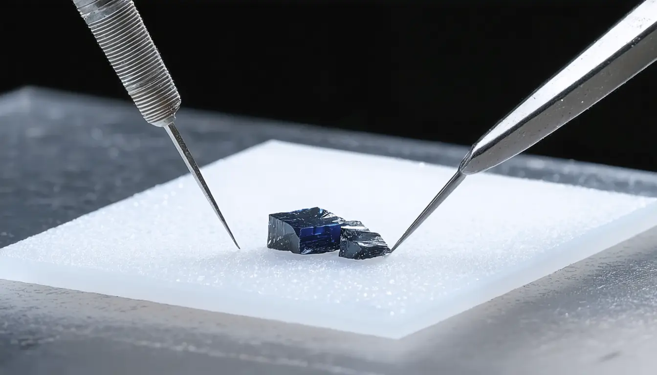
A 61.3 millivolt change in gate voltage raised current tenfold in the WSe2 transistors. The theoretical room-temperature limit is about 60 millivolts per decade. The gate oxide, converted from the crystal's upper layers, has an effective thickness below 1 nanometer.
| Figure | Value | Note | Claim |
|---|---|---|---|
| Gate voltage change for a tenfold current rise | 61.3 millivolts | 12 | |
| Theoretical limit, about | 60 mV per decade | 12 | |
| Oxide thickness, below | 1 nm, effective | 11 |
What happened
- The top layers of the WSe2 crystal were oxidized to insulating oxide, and vapor-phase reactions turned parts of it into an n-type semiconductor or a semimetal.
- The oxide above the channel served as the gate dielectric with an effective thickness under 1 nanometer, and no separate high-k material was deposited.
- Reaction temperature and gas pressure set how many layers converted, with control at roughly 0.7 nanometers per monolayer.
- The work, led by Jo Moon-Ho at IBS's Center for Van der Waals Quantum Solids, is published in Science.
Why it matters
- What's now possible capability A gate dielectric grown from the channel itself removes the deposition step where uniform coverage on a 2D surface has been hardest to get.
- Who has to decide decision Groups choosing an integration route for 2D devices now have in-place conversion to weigh against metal deposition and mechanical transfer.
- What it limits constraint Production relevance depends on uniform conversion over large areas.
- Who's exposed exposure A swing within about 2 percent of the limit shows the gate stack works. The contacts, which the same process also has to supply, are a separate question.
The 61.3 millivolt figure sits about 1.3 millivolts above the roughly 60 millivolts per decade room-temperature limit, a gap of about 2 percent [13]. That is a strong result for a gate stack, and it came from an oxide formed out of the channel's own upper layers [11][12].
The design answers a specific list of failures. According to the phys.org account of the work, the surfaces of 2D semiconductors have few sites where other materials can attach, so conventional dielectrics are hard to deposit uniformly [4]. Deposited metals can damage the atomically thin semiconductor or create large contact barriers [5]. Peeling and stacking separate 2D materials avoids both problems, but those transfer methods are difficult to scale uniformly over large areas and poorly suited to mass production [6].
Converting layers in place removes the step where a foreign material has to land on a hard-to-wet surface. The tungsten framework stays intact while the surrounding atoms are swapped, so every region shares a parent lattice [7]. We think that shared lattice is the real design choice here, and the one a reviewer would press on.
Jo said of the motivation: "One of the central challenges in two-dimensional semiconductor research has not simply been finding better semiconductors, but securing equally suitable dielectrics and electrical contacts." [10]
The account of the paper available to us gives no contact-resistance or large-area data, and no device counts or sample size. That single write-up is our only source. The production bottleneck, by the account above, is uniformity across large areas [6]. Reaction temperature and gas pressure are the controls the team used to stop conversion at a chosen layer [9], and those are the quantities a large-area test would have to hold steady.
What to watch
- Whether the team or others report contact resistance for the converted semimetal regions.
- Conversion-depth data across a wafer or a large area, which would show if the temperature and pressure recipe holds uniformly.
- Independent groups reproducing the sub-1-nanometer oxide and the near-limit switching on their own WSe2 crystals.
Clarity's read
What the record supports and how the coverage leans. The claims behind it follow.
Reality
- Evidence62
- Adoption
- Insufficient
- Hype gap+15
- Incentives
- Insufficient
- Confidence55
Claim ledger
Ranked by verification strength, evidence, and original report placement.
- [1]
A transistor normally requires a semiconductor to carry current, an insulating dielectric to control it and metallic contacts; integrating these components gets harder as devices approach the atomic scale.
- [2]
A team led by Director Jo Moon-Ho of the Center for Van der Waals Quantum Solids at the Institute for Basic Science published the work in the journal Science.
- [3]
Instead of fabricating the semiconductor, dielectric and contact materials separately and assembling them, the researchers started from a single layered crystal and chemically converted selected atomic layers and regions into the different materials needed for a working transistor.
- [4]
The surfaces of 2D semiconductors contain few sites where other materials can readily attach, which makes it difficult to deposit conventional dielectric materials uniformly.
- [5]
Direct deposition of metals can damage the atomically thin semiconductor or create large contact barriers that reduce device performance.
- [6]
Mechanical transfer methods, in which separate 2D materials are peeled, positioned and stacked one by one, are difficult to scale uniformly over large areas and remain poorly suited to mass production.
- [7]
The team began with multilayer tungsten diselenide (WSe2) and, by preserving the tungsten framework while selectively replacing surrounding atoms, changed the electronic character of individual regions without rebuilding the whole crystal.
- [8]
The upper WSe2 layers were first oxidized into insulating tungsten oxide, which vapor-phase reactions could convert into tungsten disulfide (an n-type semiconductor) or tungsten ditelluride (a semimetal); unconverted regions kept the WSe2 semiconductor character.
- [9]
Tiny gaps between neighboring atomic layers helped control how far the reaction spread; by adjusting reaction temperature and gas pressure the team stopped conversion after a chosen number of layers, with control at roughly 0.7 nanometers per WSe2 monolayer.
- [10]
Jo said, "One of the central challenges in two-dimensional semiconductor research has not simply been finding better semiconductors, but securing equally suitable dielectrics and electrical contacts."
- [11]
Converting the upper WSe2 layers directly above the channel into tungsten oxide produced a gate dielectric without depositing a separate high-k material, with an effective thickness below 1 nanometer while maintaining strong insulating performance.
- [12]
In the fabricated WSe2 transistors, a change of only 61.3 millivolts in gate voltage increased the current tenfold, very close to the theoretical room-temperature limit of about 60 millivolts per decade.
- [13]
The reported 61.3 mV per decade is about 1.3 mV, or roughly 2 percent, above the roughly 60 mV per decade room-temperature limit.
Get this ledger inside ChatGPT. Ask about any of our stories and the answer brings its figure, each claim’s verdict and the sources. Free, no account.
Sources
1 independent publisher whose own reporting we read for this story.
- phys.orgSingle 2D crystal transforms into transistor with built-in insulation and electrical contacts
1 article · October 15, 2026
Topics and entities
Follow any of these and your For You feed starts watching them — no settings page required.