KAIST team places single MoS2 crystals at chosen sites across 400 patterns
A KAIST-led team grew a single MoS2 crystal at its assigned site in over 99% of 400 patterned regions, per a Nature paper. The team has not built a stacked processor or measured any speed or energy gain.
The Product Desk
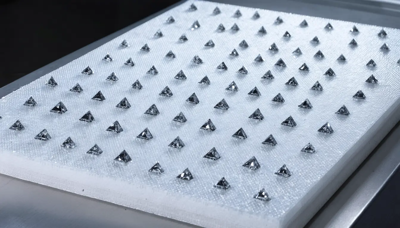
At most 3 patterns missed, out of 400 patterns reported. If the under-1% miss rate held across 1,000 sites, fewer than 10 sites would miss; this is illustrative, not a reported figure.
| Figure | Value | Note | Claim |
|---|---|---|---|
| Patterns missed, at most | 3 patterns | 16 | |
| Patterns reported | 400 patterns | 2 | |
| Missed sites per 1,000 if rate held, fewer than | 10 sites | Illustrative, not a reported figure | 17 |
What happened
- The method, called EF-SCN, rings each growth region with an oxide barrier such as hafnium oxide that releases oxygen to suppress unwanted crystals.
- Oxygen's etching effect is strongest at the edges of a patterned region and weakens toward the center, so crystals tend to start at one central point.
- In structures combining MoS2 and MoSe2, a thin ruthenium film formed only on the MoSe2 regions, a second demonstration of controlled material placement.
- UNIST, Hanyang University and TDS Innovation worked with KAIST on the method.
Why it matters
- capability If direct growth holds up, fabs could skip the step of making 2D material separately and transferring it onto a chip.
- exposure A miss rate under 1% still means fewer than 10 failed sites per 1,000, and the reported run covers only 400 patterns.
- constraint Stacked chips need growth on surfaces that already hold circuits, so the placement result has to be repeated under that condition before it counts toward a schedule.
- decision Teams tracking 2D materials can log this as placement evidence now and hold any speed or energy case until someone measures it.
Take the process engineer who has patterned a growth region for MoS2 and wants exactly one crystal in it. Conventional methods can define the general area where a thin film forms, but the exact starting point of each crystal is hard to control [3]. When several crystals start independently and meet, they form grain boundaries that disrupt the regular arrangement of atoms and can interfere with the movement of electrons [4].
Two-dimensional semiconductors keep their properties at a few atomic layers [9], so compute and memory could stack vertically with shorter data paths, and moving data inside a chip costs energy and time [15]. The experiment itself put one crystal at the designated center in more than 99% of 400 patterns [2]. That count allows at most 3 misses [16].
Once growth begins at the center, the process suppresses additional crystals from forming nearby [7]. A second crystal is how a grain boundary forms [4], so that suppression is what a fab would need to see hold across many sites.
A miss rate under 1% sounds small. If it held across 1,000 sites, fewer than 10 would still fail the single-crystal test [17]. The study, published October 8 in Nature [14], reports one count, 400 patterns. The coverage does not say whether they were grown over fabricated circuits, the condition stacked chips require [10].
According to Interesting Engineering, the technique offers a possible way to grow high-quality 2D material directly at designated locations. That would remove the step of manufacturing it separately and transferring it onto a chip [11]. The same report says further development would be needed to learn whether the method can be integrated into semiconductor manufacturing at scale [13].
In our view, this is for process-integration and R&D leads weighing 2D materials for stacked designs; product teams with a ship date come later.
A two-by-two grid sorts any result like this one. One axis is what was measured: where crystals landed, or how a finished chip performed. The other is where the growth happened: on patterned regions, or on top of fabricated circuits [10]. The coverage puts this paper in the first cell, crystal placement counted across patterned growth regions [2]. A stacked-chip schedule depends on the cells where performance is measured over fabricated circuits. Until a study fills those, the result belongs on the research watch list.
What to watch
- A follow-up showing single-crystal placement on surfaces that already hold fabricated circuits.
- A stacked processor, or any measured speed or energy figure, built with the method.
- A success rate reported across far more than 400 patterns.
Clarity's read
What the record supports and how the coverage leans. The claims behind it follow.
Reality
- Evidence62
- Adoption
- Insufficient
- Hype gap+12
- Incentives
- Insufficient
- Confidence60
Claim ledger
Ranked by verification strength, evidence, and original report placement.
- [1]
A team led by KAIST worked with UNIST, Hanyang University and TDS Innovation to develop the method.
- [2]
The researchers grew individual MoS2 crystals at designated central positions in more than 99% of 400 patterns.
- [3]
Conventional semiconductor growth methods can define the general area where a thin film forms, but controlling the exact starting point of each crystal remains difficult.
- [4]
When several crystals grow independently and meet, they create grain boundaries that disrupt the regular arrangement of atoms and can interfere with the movement of electrons through the semiconductor.
- [5]
The process, called etching-flux-mediated single-centered nucleation (EF-SCN), uses an oxide barrier such as hafnium oxide (HfO2) surrounding the designated growth region; oxygen released from the barrier acts as an etching agent that suppresses unwanted crystal formation.
- [6]
The oxygen's effect is strongest near the edges of the patterned region and gradually weakens toward the center, creating conditions that favor crystal formation at a single central point.
- [7]
Once growth begins at the central point, the process also suppresses additional crystals from forming nearby.
- [8]
In structures combining MoS2 and MoSe2, a thin ruthenium metal film formed selectively on the MoSe2 regions, demonstrating another way to control material placement during semiconductor fabrication.
- [9]
Two-dimensional semiconductors retain semiconductor properties despite being only a few atomic layers thick, and their small thickness could allow manufacturers to stack computing and memory components vertically, reducing the distance data travels between them.
- [10]
Producing stacked chips requires precise control over semiconductor growth on surfaces containing previously fabricated circuits.
- [11]
The KAIST technique offers a possible way to grow high-quality 2D materials directly at designated locations, avoiding the need to manufacture them separately and transfer them onto a chip.
- [12]
The researchers have not demonstrated a complete stacked processor or measured improvements in computing speed or energy consumption.
- [13]
Further development would be needed to determine whether the method can be integrated into semiconductor manufacturing at scale.
- [14]
The study was published October 8 in Nature.
- [15]
Moving data within a chip consumes energy and contributes to processing delays.
- [16]
More than 99% of 400 patterns is more than 396 successes, so at most 3 patterns missed.
- [17]
If the under-1% miss rate held across 1,000 sites, fewer than 10 sites would miss (illustrative scale, not a reported figure).
Sources
1 independent publisher whose own reporting we read for this story.
- interestingengineering.comOxygen-based chipmaking method controls 2D crystal growth with over 99% success
1 article · October 13, 2026
Topics and entities
Follow any of these and your For You feed starts watching them — no settings page required.
Topics
- Vertically stacked chipsFollow
- 2D semiconductorsFollow
- Semiconductor manufacturing and packagingFollow