ScienceNot yet confirmed elsewhere1 publisher2 min readPublished
Silicon-doped oxide films grown on sapphire conduct at bandgaps above 7 eV
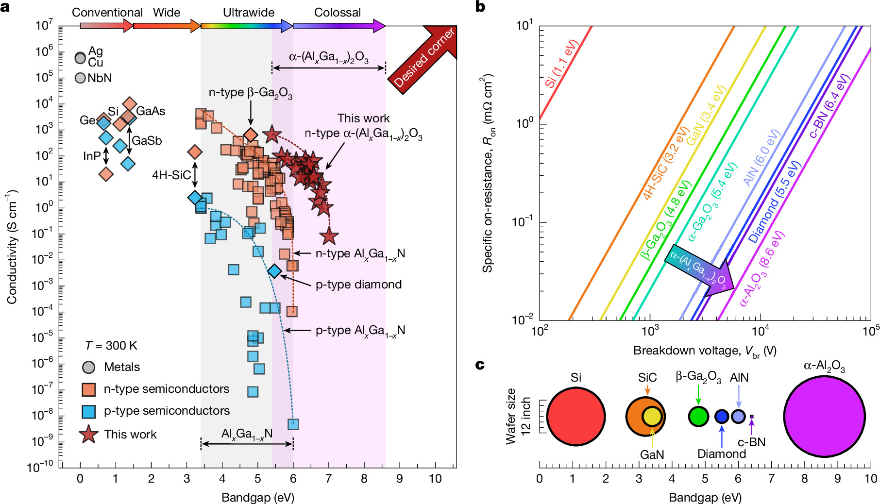
Researchers in Nature report silicon-doped oxide films on sapphire that conduct at bandgaps above 7.0 eV, wider than cubic boron nitride's. Doping is the hard part at such gaps, so the result gives ultra-wide-bandgap power devices an oxide candidate to weigh against boron nitride.
The Scientist · Science desk
What happened
- In the range above 6 eV, the films conduct at room temperature more than 100 million times better than any earlier report, according to the authors.
- The team built a Schottky diode and a field-effect transistor, named the AlphaFET, with channels in that above-6 eV range.
- A 2020 report the paper cites had made conductive silicon-doped films of the same alloy with bandgaps up to 6.22 eV.
Why it matters
- capability Device groups can now test power-device scaling at gaps wider than cubic boron nitride's in a material whose conductivity can be set by doping.
- cost Substrate cost would sit with sapphire, which the authors call inexpensive and made at massive scale, and away from the difficult, costly, small-format synthesis they attribute to diamond and cubic boron nitride.
- precedent If the doping holds up, the alloy joins GaN, SiC, AlN, Ga2O3 and GeO2 as former insulators that became semiconductors once defects fell and the right dopant was found.
Growing this alloy with a very wide gap was already possible. A 2021 study the paper cites grew alpha-(AlGa)2O3 spanning 5.4 to 8.6 eV on m-plane sapphire [12]. The advance is in the doping [1]. As the bandgap increases, the authors write, the ability to modulate a semiconductor's conductivity over orders of magnitude by equilibrium doping "becomes increasingly elusive" [4].
The 100-million-fold conductivity figure has a specific denominator. The "previous reports" it is measured against are cited to a 2024 study of silicon-doped alpha-(AlGa)2O3 grown by MOCVD on m-plane sapphire [2]. So the factor measures how far doping above 6 eV has come relative to earlier films in that same range [1].
The authors frame the payoff with the Baliga figure of merit, which they give as proportional to the bandgap raised to the 5.5th power [3]. Taking the 6.22 eV conductive films of the 2020 report as a starting point [11], a move to 7.0 eV [6] raises that figure about 1.9-fold on the scaling rule alone [14]. That is an estimate from bandgap. The abstract does not report the films' absolute conductivity, or the breakdown voltage and current of the Schottky diode or the AlphaFET.
The authors' cost argument is about the wafer [15], but production cost also depends on the growth step. A 2024 paper the authors cite reported growing this alloy by suboxide molecular-beam epitaxy at 1 micrometre per hour [13].
I think the oxide route has the stronger claim on scale, and its claim on performance is still open. The authors' case against diamond and cubic boron nitride rests on synthesis difficulty, cost and small size [16], and none of those depends on how the AlphaFET performs.
What to watch
- Breakdown voltage, on-resistance and current figures for the AlphaFET and the Schottky diode, which would show whether the Eg^5.5 scaling survives in real devices.
- A second group reproducing above-6 eV conductivity, for instance by MOCVD, the growth method behind the 2024 baseline the paper compares against.
- Doped films at higher aluminium content, which would show how far above 7 eV the method extends.
Clarity's read
What the record supports and how the coverage leans. The claims behind it follow.
Reality
- Evidence55
- Adoption
- Insufficient
- Hype gap+20
- Incentives
- Insufficient
- Confidence50
Claim ledger
Ranked by verification strength, evidence, and original report placement.
- [1]
In the colossal-bandgap regime, above 6 eV, the silicon-doped films have room-temperature conductivities over 100 million times higher than all previous reports.
- [2]
The 'all previous reports' conductivity comparison is cited to a 2024 study (Okumura and Varley) of MOCVD growth of Si-doped alpha-(AlGa)2O3 on m-plane sapphire substrates.
- [3]
In rectifying power electronics, wider-bandgap semiconductors allow higher efficiency and power density, with the Baliga figure of merit proportional to Eg^5.5.
- [4]
The ability of semiconductors to have their conductivities controllably modulated over orders of magnitude by equilibrium doping methods becomes increasingly elusive as the bandgap increases.
- [5]
GaN, SiC, AlN, Ga2O3 and GeO2, previously considered insulators, emerged as useful semiconductors after defect densities were decreased and appropriate dopants were found.
- [6]
The silicon-doped alpha-(AlxGa1-x)2O3 films have bandgaps exceeding 7.0 eV.
- [7]
The films' bandgap surpasses that of cubic boron nitride, the next-widest-bandgap semiconductor known.
- [8]
The researchers fabricated a Schottky diode and a field-effect transistor, the AlphaFET, with colossal-bandgap (above 6 eV) channels.
- [11]
The paper cites a 2020 AIP Advances report (Dang et al.) of conductive Si-doped alpha-(AlxGa1-x)2O3 thin films with bandgaps up to 6.22 eV.
- [12]
The paper cites a 2021 Science Advances study (Jinno et al.) of epitaxy of 5.4 to 8.6 eV alpha-(AlGa)2O3 on m-plane sapphire.
- [13]
The paper cites a 2024 APL Materials report (Steele et al.) of epitaxial growth of alpha-(AlxGa1-x)2O3 by suboxide molecular-beam epitaxy at 1 micrometre per hour.
- [14]
Under the stated Eg^5.5 scaling, a 7.0 eV bandgap gives a Baliga figure of merit about 1.9 times that of a 6.22 eV bandgap.
- [15]
The films and devices use sapphire, which the authors describe as an abundant, inexpensive substrate with excellent quality that is produced at massive scale.
- [16]
The authors say the achievement breaks the trend of increasing synthesis difficulty, cost and small size of ever-wider-bandgap semiconductors, for example diamond and cubic boron nitride.
Sources
1 independent publisher whose own reporting we read for this story.
Topics and entities
Follow any of these and your For You feed starts watching them — no settings page required.