BuildNot yet confirmed elsewhere1 publisher3 min readPublished
NVIDIA and Cisco propose USFP, an OSFP-sized optic with 16 lanes at 400Gb/s each
NVIDIA and Cisco announced plans for USFP, a pluggable optic with 400Gb/s per lane and a stated ceiling of 12.8Tb/s per module. The first planned modules have 16 lanes, or 6.4Tb/s each way, so the ceiling needs 32 lanes or a two-way count.
The Engineer · Build desk
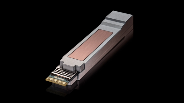
Four figures NVIDIA and Cisco state for USFP: 4x the front-panel bandwidth density of 200Gb/s-per-lane pluggable modules; capacity up to 12.8Tb/s; power dissipation up to 100 watts without a dedicated cooling circuit; lane count scaling to 32 full-duplex lanes and more.
| Figure | Value | Note | Claim |
|---|---|---|---|
| Bandwidth density vs 200Gb/s-per-lane modules | 4 x | 13 | |
| Module capacity, up to | 12.8 Tb/s | 1 | |
| Power dissipation, up to | 100 watts | 5 | |
| Lane scaling, at least | 32 duplex lanes | 4 |
What happened
- The two companies claim 4x the bandwidth density and approximately 1.3x the power efficiency of 200Gb/s-per-lane pluggable modules, measured against an OSFP-sized module.
- The module supports power dissipation of up to 100 watts without a separate, dedicated embedded cooling circuit inside the transceiver.
- TE Connectivity and Amphenol are partnering with NVIDIA and Cisco so that USFP hardware comes from more than one supplier.
Why it matters
- cost Operators pay for the density in watts per cage, so we'd expect faceplate cooling and power delivery to cap how many USFP modules a chassis can run at full rate.
- decision Teams building 200Gb/s-per-lane fabrics have to decide whether to wait for USFP cages, since the release says the same connector performs better at 200Gb/s per lane and scales to 400.
- contradiction The release promises adoption without overhauling data center infrastructure, yet the module mates through a new connector, so the host side has to change.
The first planned USFP module has 16 lanes in an OSFP-sized footprint [2]. At 400Gb/s per lane, that is 6.4Tb/s per direction [7]. The 4x claim fits that figure. The release says the design doubles both lane count and per-lane rate [12], which puts the 200Gb/s baseline at 8 lanes and 1.6Tb/s, and four times 1.6 is 6.4 [15].
The 12.8Tb/s ceiling [1] takes 32 lanes at 400Gb/s [8]. The connector is designed to allow 32 lanes [4], but the first module is not that part. The other reading is that 12.8Tb/s counts both directions of a full-duplex 16-lane module. The release does not say which basis it uses.
The motivation is switch radix. According to the release, when a switch reaches capacity, further expansion can require more switch layers and optical links, which adds latency, power and cost [14]. The pitch is more 1.6Tb/s endpoints per switch without another tier [12]. Cisco's Bill Gartner, senior vice president and general manager of optical systems and optics, put the goal in operational terms. "AI builders need an interconnect architecture that can scale performance without locking them into a more complex operating model," he said [10].
Power needs a closer look. The 1.3x figure is per bit. If it means bits moved per watt, a module with 4x the bandwidth at 1.3x the efficiency draws about 3.1 times the power of the 200Gb/s module at full rate, since 4 divided by 1.3 is 3.08 [9]. The release puts the dissipation ceiling at 100 watts, with no separate, dedicated embedded cooling circuit inside the transceiver [5].
The connector is the new part. USFP mates through a two-dimensional array connector with a two-step insertion that engages the high-speed contacts after the module is inserted [3]. The release credits that with less contact wear, better signal integrity and more predictable insertion force [3]. Because it is built for 400Gb/s, it also performs better at 200Gb/s per lane [4].
A module that takes 400Gb/s electrical lanes needs a host that supplies them, and a new connector needs a cage that has it. We'd expect new cage hardware on every switch and SuperNIC that takes USFP. That sits against the release's line that customers can adopt it "without overhauling their data center infrastructure" [11]. TE Connectivity and Amphenol are working with NVIDIA and Cisco on the multi-source ecosystem [6].
The figures are the two vendors' own, from NVIDIA's announcement [13]. For the 1.3x to hold on a given fabric, the 200Gb/s-per-lane module it replaces would have to be the same optic type and reach, and the switch and SuperNIC silicon would have to drive 400Gb/s electrical lanes at no extra power penalty.
What to watch
- Connector and cage specifications from TE Connectivity and Amphenol, and whether other vendors join the ecosystem.
- A datasheet that states how 12.8Tb/s is counted and which 200Gb/s-per-lane module the 1.3x is measured against.
- Switch and SuperNIC silicon with 400Gb/s electrical lanes that can drive the module.
Clarity's read
What the record supports and how the coverage leans. The claims behind it follow.
Reality
- Evidence25
- Adoption
- Insufficient
- Hype gap+30
- Incentives70
- Confidence55
Claim ledger
Ranked by verification strength, evidence, and original report placement.
- [1]
NVIDIA and Cisco describe USFP as designed to be the first module to support 400Gb/s-per-lane electrical signals, with capacity up to 12.8Tb/s.
- [2]
The first planned USFP-based transceivers pack 16 full-duplex lanes in an OSFP-sized footprint supporting both switches and SuperNICs, with the ability to expand to 32 and more lanes in the future.
- [3]
USFP uses a new two-dimensional array connector with a two-step insertion design that engages high-speed contacts after the module is inserted, reducing contact wear, improving signal integrity and making insertion force more predictable.
- [4]
The connector technology allows scaling of lane count to 32 full-duplex lanes and more, and because it is designed for 400Gb/s performance it also offers improved performance at 200Gb/s per lane.
- [5]
USFP supports power dissipation of up to 100 watts without needing a separate, dedicated embedded cooling circuit within the transceiver.
- [6]
NVIDIA and Cisco are working with TE Connectivity and Amphenol to build a multi-source hardware ecosystem around USFP.
- [7]
16 lanes at 400Gb/s each is 6,400Gb/s, or 6.4Tb/s per direction.
- [8]
A 12.8Tb/s module at 400Gb/s per lane needs 32 lanes.
- [9]
If power efficiency means bits moved per watt, a module with 4x the bandwidth at 1.3x the efficiency draws about 3.1 times the power of the 200Gb/s module at full rate.
- [10]
"AI builders need an interconnect architecture that can scale performance without locking them into a more complex operating model," said Bill Gartner, senior vice president and general manager of optical systems and optics at Cisco.
ReportedContestedSource: Bill Gartner, Cisco2 sources— create a free account to open themView cited source - [11]
The release says customers can meet the performance demand of AI workloads with USFP "without overhauling their data center infrastructure."
ReportedContestedSource: NVIDIA and Cisco announcement2 sources— create a free account to open themView cited source - [12]
The release says doubling both the lane count and the bandwidth per lane lets AI fabrics connect more 1.6Tb/s endpoints without adding network tiers.
- [13]
Compared with an OSFP-sized module, USFP delivers 4x the bandwidth and front-panel bandwidth density, with approximately 1.3x the power efficiency, versus 200Gb/s-per-lane pluggable modules.
- [14]
When a switch reaches its capacity, further network expansion can require additional switch layers and optical links, increasing latency, power consumption and costs.
- [15]
If USFP doubles lane count and lane rate, the OSFP baseline is 8 lanes at 200Gb/s, or 1.6Tb/s, and 4x that is 6.4Tb/s, matching the 16-lane 400Gb/s figure.
Sources
1 independent publisher whose own reporting we read for this story.
- nvidianews.nvidia.comNVIDIA and Cisco Introduce New Pluggable Optics Form Factor to Scale AI Factories
1 article · October 12, 2026
Topics and entities
Follow any of these and your For You feed starts watching them — no settings page required.
Topics
- Pluggable opticsFollow
- AI Data Center NetworkingFollow