Intel's EMIB bridges are heading to a 25-micron bump pitch
Intel's recent roadmaps take EMIB's bump pitch from 45 microns to about 36 and then 25, Tom's Hardware reports. Virtually all its high-end client and data center CPUs already rely on EMIB and Foveros, but 12-reticle packages remain a goal.
The Engineer · Build desk
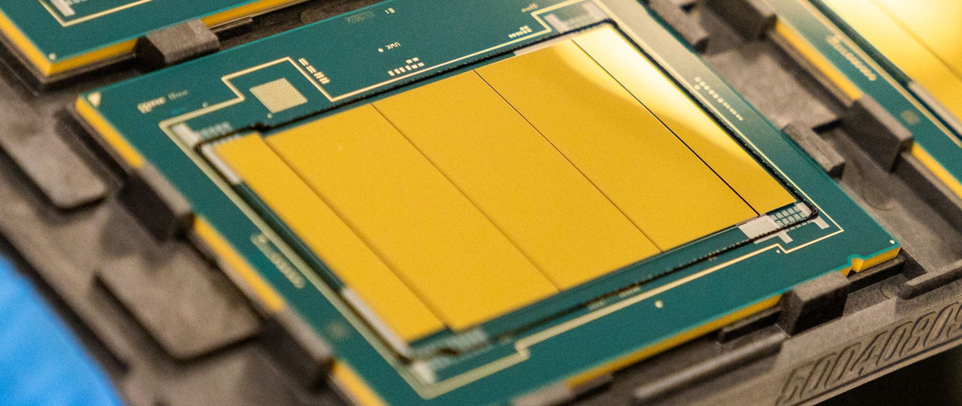
Three figures for EMIB bump pitch: early EMIB used a 55-micron first-layer bump pitch, Intel later reduced it to 45 microns, and Intel's recent roadmaps show a next step to around 36 microns, before ultimately 25 microns.
| Figure | Value | Note | Claim |
|---|---|---|---|
| Early EMIB first-layer bump pitch | 55 microns | 4 | |
| Pitch Intel reduced it to | 45 microns | 4 | |
| Roadmap's next pitch | 36 microns, around | 5 |
What happened
- EMIB entered high-volume manufacturing in 2017 as a way to connect adjacent chiplets without an expensive silicon interposer.
- EMIB-M puts metal-insulator-metal capacitors inside the bridge to improve power delivery and suppress voltage fluctuations close to the compute dies.
- EMIB-T adds through-silicon vias, so power travels vertically through the bridge instead of taking longer paths around it.
- Tom's Hardware says EMIB and Foveros no longer look like two mostly separate technologies and in many cases complement each other.
Why it matters
- capability EMIB is set to enable AI accelerators 12 reticles across, with dozens of bridges and more than 24 HBM stacks.
- constraint Multi-kilowatt packages with HBM4-class memory are limited by current density and power integrity, and the capacitor and through-silicon-via bridges aim at those limits.
- cost Simpler EMIB and Foveros variants for cost-sensitive products mean the packaging is not confined to the most expensive parts.
EMIB embeds small silicon bridges in an organic package substrate, and only where high-density die-to-die connectivity is required. [3] The rest of the package uses conventional substrate wiring and relaxed bump pitches. [3] A finer pitch on the bridge puts more connections along a chiplet's edge, the quantity Tom's Hardware calls shoreline density. [6] It also raises the interconnect density that bigger system-in-packages need. [18]
Early parts used a 55-micron pitch. [4] The steps Tom's Hardware lists give gains of about 1.22 times for 55 to 45, 1.25 times for 45 to 36, and 1.44 times for 36 to 25. [21] [22] [20] Each step is bigger than the one before it. End to end, 55 to 25 is 2.2 times as many connections along the same edge, if the number of bump rows stays the same. [19] Neither the 36-micron nor the 25-micron step comes with a date.
The bridges also address power delivery. EMIB-M addresses the power-integrity problem that big processors create, and Tom's Hardware names Xeon 6 "Granite Rapids" as one. [14] EMIB-T, it says, also simplifies power routing, lowers impedance and reduces noise. [15] In our view, the density gain reaches a product only when the dies on both sides of a bridge are designed for the finer pitch.
The Foveros side is thin. The one concrete item is that the 12-reticle goal pairs EMIB with Foveros Direct 3D. [10]
After what Tom's Hardware calls the "fiasco" with Intel's initial 10nm process, the company made clear that its multi-chiplet strategy was a sustainable way to deliver performance and features cost-efficiently at a predictable cadence. [17] The article concedes that not every multi-chiplet project succeeded. Most recent client and data center CPUs still use several chiplets and rely on EMIB and Foveros. [16]
What to watch
- Dates for the 36-micron and 25-micron bump pitch steps, which the material reviewed does not give.
- Which Intel parts adopt EMIB-T's through-silicon vias for HBM4-class memory.
- Whether Intel shows EMIB combined with Foveros Direct 3D at the 12-reticle scale.
Clarity's read
What the record supports and how the coverage leans. The claims behind it follow.
Reality
- Evidence55
- Adoption50
- Hype gap+20
- Incentives55
- Confidence60
Claim ledger
Ranked by verification strength, evidence, and original report placement.
- [1]
Virtually all of Intel's high-end client and data center CPUs rely on its EMIB and Foveros technologies.
- [2]
EMIB entered high-volume manufacturing in 2017 as a relatively straightforward way to connect adjacent chiplets without using an expensive silicon interposer.
- [3]
EMIB embeds tiny silicon bridges into an organic package substrate only where high-density die-to-die connectivity is required, and the rest of the package uses conventional substrate wiring and relaxed bump pitches.
- [4]
Early EMIB implementations used a 55-micron first-layer-interconnect (FLI) bump pitch, which Intel subsequently reduced to 45 microns.
- [5]
Intel's recent roadmaps indicate further EMIB bump pitch reductions to around 36 microns and ultimately 25 microns.
- [6]
Reducing the bump pitch dramatically increases the number of connections that can fit along a chiplet's edge (shoreline density).
- [7]
EMIB-M incorporates metal-insulator-metal (MIM) capacitors into the bridge to improve power delivery and suppress voltage fluctuations close to compute dies.
- [8]
EMIB-T adds through-silicon vias (TSVs) to the bridge, which let power travel vertically through it instead of taking longer paths around it.
- [9]
For multi-kilowatt system-in-packages and HBM4-class memory subsystems, current density and power integrity are major packaging constraints.
- [10]
Intel's ultimate goal is to build system-in-packages the size of 12 reticles using both EMIB and Foveros Direct 3D, but it is not quite there yet.
- [11]
EMIB is set to enable massive AI accelerators 12 times the size of a reticle, with dozens of silicon bridges, more than 24 HBM stacks and advanced power delivery.
- [12]
As the roadmap evolves, EMIB and Foveros become more sophisticated for demanding products and also simpler to cover cost-sensitive products.
- [13]
EMIB and Foveros no longer seem to be two mostly separate technologies; in many cases they complement each other and Intel's upcoming process technologies.
- [14]
EMIB-M addresses the power-integrity problem created by big processors, such as Intel's Xeon 6 'Granite Rapids'.
- [15]
EMIB-T simplifies power routing, lowers impedance and reduces noise.
- [16]
Not all of Intel's multi-chiplet projects were a success, but the majority of its client and data center CPU products launched in recent years use multiple chiplets and rely on EMIB and Foveros.
- [17]
Following the fiasco with its initial 10nm process technology, Intel made clear that its multi-chiplet strategy is a sustainable way to deliver performance and feature enhancements cost-efficiently at a predictable cadence.
- [18]
A finer FLI pitch increases the interconnect density required to build bigger system-in-packages.
- [19]
Going from a 55-micron to a 25-micron bump pitch gives about 2.2 times as many connections along the same chiplet edge, assuming the same number of bump rows.
- [20]
The step from a 36-micron to a 25-micron pitch is a gain of about 1.44 times in edge density.
- [21]
The step from a 55-micron to a 45-micron pitch is a gain of about 1.22 times in edge density.
- [22]
The step from a 45-micron to a 36-micron pitch is a gain of about 1.25 times in edge density.
Get this ledger inside ChatGPT. Ask about any of our stories and the answer brings its figure, each claim’s verdict and the sources. Free, no account.
Sources
1 independent publisher whose own reporting we read for this story.
- tomshardware.comAnalyzing Intel's EMIB and Foveros advanced packaging roadmaps
1 article · October 14, 2026
Topics and entities
Follow any of these and your For You feed starts watching them — no settings page required.