MediaTek will wire custom XPUs into NVIDIA's scale-up fabric as a prevalidated block
NVIDIA is licensing the Fusion chiplet, its C2C CPU attach and NVHBM to MediaTek and buying $3.5 billion of its convertible bonds, so the quickest route to a custom accelerator now ends inside an NVIDIA rack.
The Engineer · Build desk
What happened
- MediaTek will adopt NVIDIA's NVLink Fusion platform, offering hyperscalers, cloud providers and frontier model developers a prevalidated route for custom XPUs into NVLink-connected rack-scale AI factories.
- NVIDIA has separately invested $3.5 billion in convertible bonds issued by MediaTek, disclosed in the same announcement as the licensing arrangement.
- MediaTek will sell the platform as the design foundation for customer accelerators, which NVIDIA says lets those platforms evolve alongside its future architectures.
- The two companies also continue joint work on multiple generations of RTX Spark and DGX Spark PC chips that pair NVIDIA GPUs with MediaTek SoCs for PCs, developer machines and workstations.
Why it matters
- Who has to decide decision A custom-silicon team now chooses between owning chip-to-rack engineering and qualification itself or buying that work from the vendor its accelerator was commissioned to route around.
- What it limits constraint Sitting on a foundation that tracks NVIDIA's architecture roadmap makes an XPU program's generation cadence a scheduling dependency on NVIDIA, not only a technical one.
- What's now possible capability A design house with compute IP but no in-house SerDes, HBM or rack integration muscle can attempt a production accelerator without first building those teams.
- Who's exposed exposure MediaTek's custom-silicon customers hand their designs to a partner whose bondholder is NVIDIA, on conversion terms the announcement leaves unstated.
The component list matters most at the interface level, and that is where the design decision actually sits.
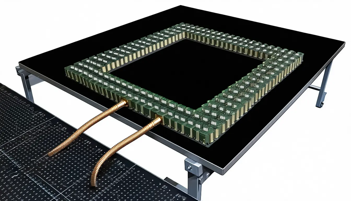
NVIDIA names a Fusion chiplet that attaches a customer XPU to the NVLink scale-up fabric over NVIDIA photonics or electrical interconnects [10]. It names NVLink-C2C for high-bandwidth connection to NVIDIA Rosa CPUs and other compatible processors [11]. It names NVHBM for customised memory, which the release says increases bandwidth and frees silicon area for compute [12]. Those are the three external edges of an accelerator: how it talks to peers, how it talks to a host, how it reaches memory. What is left for the customer is the compute die [17].
The same release supplies two lists that are worth putting side by side. In one, customers rely on NVIDIA and MediaTek for NVLink connectivity, memory architecture, packaging, manufacturing and rack-scale technologies [15]. In the other, customers bring an XPU design to MediaTek and tailor connectivity, memory, packaging, performance and power [16]. Three of the five tailorable items are the same three items being supplied [18]. Tailoring here means parameterising inside someone else's blocks.
The invisible constraint is stated plainly: getting from multi-die silicon to a manufacturable rack requires SerDes, HBM, I/O, scale-up networking, qualification and supply-chain support [14]. Any team that taped out an accelerator and then discovered the rack was the hard part will recognise the pitch, because it is written for them.
"Prevalidated" [8] is a claim about somebody else's integration work, and it only transfers under conditions the release does not enumerate. The packaging flow has to be one MediaTek has already qualified, the memory has to be NVHBM rather than a stack negotiated independently [12], and the scale-up topology has to be NVLink's [10] -- so if your accelerator's advantage comes from a different fabric or a different collective, the prevalidated foundation stops saving you time. The sentence to underline is that platforms will evolve alongside future NVIDIA architectures [4]. Read as a schedule rather than a feature, that couples your generation cadence to NVIDIA's.
The financing carries the least published detail. NVIDIA bought $3.5 billion of convertible bonds issued by MediaTek [3], and the announcement gives no conversion price, coupon or maturity [13]. MediaTek chief executive Rick Tsai said the investment strengthens a collaboration spanning cloud AI infrastructure, local AI computing and automotive [6]. Jensen Huang framed the result as giving customers freedom to create differentiated AI systems at scale [5].
Custom XPU programs exist because large buyers wanted a part they controlled. The route to production now on offer keeps the compute die theirs [2] and moves fabric, host attach, memory architecture, packaging and rack integration into NVIDIA's stack [15]. That trades time-to-rack for a narrower form of independence: the compute die is customer-owned, and everything around it now runs on NVIDIA's stack.
What to watch
- Whether a named hyperscaler commits an XPU program to the Fusion foundation, and whether it pairs with NVIDIA Rosa CPUs or its own host silicon.
- Publication of what "prevalidated" covers: which packaging flows, SerDes lanes and HBM stacks are inside the qualified matrix.
- MediaTek filings that put a conversion price, coupon and maturity on NVIDIA's $3.5 billion convertible position.
Clarity's read
What the record supports and how the coverage leans. The claims behind it follow.
Reality
- Evidence55
- Adoption20
- Hype gap+30
- Incentives80
- Confidence60
Perspective Coverage
3 publishers- Builder
- Builder 37%
- Operator
- Operator 22%
- Investor
- Investor 41%
Claim ledger
Ranked by verification strength, evidence, and original report placement.
- [1]
NVIDIA and MediaTek announced a deepening of their collaboration spanning AI infrastructure, local AI computing and automotive.
- [2]
MediaTek will adopt the NVIDIA NVLink Fusion platform to provide hyperscalers, cloud service providers and frontier model developers with a prevalidated path to develop custom XPUs and bring them into NVIDIA NVLink-connected, rack-scale AI factories.
- [3]
NVIDIA has invested $3.5 billion in convertible bonds issued by MediaTek.
- [4]
MediaTek will offer the NVLink Fusion platform as a design foundation for customers developing custom AI accelerators, enabling their platforms to evolve alongside future NVIDIA architectures.
- [5]
Jensen Huang, founder and CEO of NVIDIA, said the companies are building platforms that bring NVIDIA accelerated computing to new markets and give customers the freedom to create differentiated AI systems at enormous scale.
- [6]
Rick Tsai, vice chairman and CEO of MediaTek, said NVIDIA's investment strengthens a collaboration that spans cloud AI infrastructure, local AI computing and automotive.
- [7]
The companies will continue to collaborate on multiple generations of NVIDIA RTX Spark and DGX Spark PC chips, powering consumer PCs, AI developer supercomputers and enterprise-class workstations, integrating NVIDIA GPUs with MediaTek SoCs.
- [8]
NVIDIA says the NVLink Fusion platform provides a prebuilt, prequalified and system-prevalidated foundation for multi-die XPU development, accelerating the path from silicon and advanced packaging to rack-scale systems.
- [9]
MediaTek and NVIDIA will continue developing platforms for AI-powered, software-defined vehicles.
- [10]
The NVLink Fusion chiplet connects XPUs to the NVIDIA NVLink scale-up fabric using NVIDIA photonics or electrical interconnects.
- [11]
NVIDIA NVLink-C2C provides high-bandwidth, energy-efficient connectivity between XPUs, NVIDIA Rosa CPUs and other compatible processors.
- [12]
NVIDIA NVHBM integrates customized memory capabilities to increase bandwidth and energy efficiency while dedicating more silicon area to compute.
- [13]
The announcement states the size and instrument of the MediaTek investment but names no conversion price, coupon or maturity.
- [14]
NVIDIA states that integrating multi-die architectures, advanced packaging, high-speed SerDes, HBM, I/O and scale-up networking into a manufacturable, production-ready system requires extensive chip-to-rack engineering, qualification and supply-chain support.
- [15]
NVIDIA says customers can focus resources on differentiated compute while relying on NVIDIA and MediaTek for the NVLink connectivity, memory architecture, packaging, manufacturing and rack-scale technologies required for production deployment.
- [16]
NVIDIA says customers can bring their XPU designs to MediaTek and tailor connectivity, memory, packaging, performance and power characteristics to their workloads and infrastructure requirements.
- [17]
The three NVLink Fusion technologies NVIDIA names around a custom XPU cover all three of its external interfaces (peer fabric, host CPU attach, memory), leaving the compute die as the customer-owned surface.
- [18]
Three of the five characteristics NVIDIA says customers can tailor (connectivity, memory, packaging) are the same items NVIDIA and MediaTek supply as the prevalidated foundation.
Get this ledger inside ChatGPT. Ask about any of our stories and the answer brings its figure, each claim’s verdict and the sources. Free, no account.
Sources
3 independent publishers whose own reporting we read for this story.
- mezha.netNvidia планує інвестувати $3,5 млрд у MediaTek для розвитку ШІ-інфраструктури
1 article · August 31, 2026
- nvidianews.nvidia.comNVIDIA and MediaTek Deepen Long-Standing Partnership to Build AI Edge to Cloud Computing Platforms
1 article · August 31, 2026
- tomshardware.comNvidia pours $3.5 billion into MediaTek — company will adopt NVLink Fusion for its custom AI accelerators
1 article · September 1, 2026
Topics and entities
Follow any of these and your For You feed starts watching them — no settings page required.
Topics
- Custom AI AcceleratorsFollow
- Software-defined vehiclesFollow
- AI PCsFollow
- AI scale-up interconnectsFollow