Argonne X-rays follow a laser pulse's energy through silicon carbide in 3D
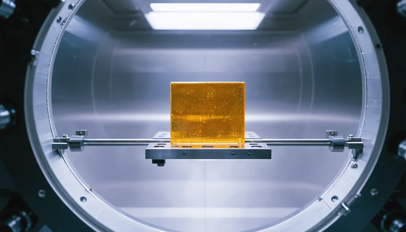
Argonne scientists using 3D, real-time X-ray imaging saw an ultrafast laser pulse's energy travel through silicon carbide in two distinct ways. Mapping that energy below the surface is groundwork for placing qubit defects exactly where engineers want them.
The Scientist · Science desk
What happened
- One of the two pathways is an organized mechanical wave that moves rapidly through the crystal, like ripples spreading over a stretched surface after it is struck.
- The laser starts the process, and precisely synchronized X-ray pulses at Argonne's Advanced Photon Source record the crystal's response over time, acting as a camera.
- The team narrowed the X-ray beam to a spot a few hundred nanometers wide, one-hundredth the width of a human hair.
- The study appears in the journal ACS Nano.
Why it matters
- capability Groups tuning laser recipes for silicon carbide defects can now check them against how the crystal responds below its surface, a region optical probes cannot easily reach.
- constraint Placing a defect where it is intended every time is still a long-term goal, so laser-written silicon carbide qubits cannot yet be positioned on demand.
- decision Labs that pick lasers over electron or ion beams for their site selection now have a way to test whether energy spreading inside the crystal works against that advantage.
Writing a qubit into silicon carbide starts with deliberate damage. An ultrafast laser pulse knocks atoms out of place, and the vacancies it leaves can behave as qubits [3]. Each pulse lasts millionths of a billionth of a second [4]. That is the femtosecond scale, 10^-15 seconds [18].
Lasers have one clear advantage over the electron and ion beams used before them: they offer the possibility of making vacancies at carefully chosen spots inside the crystal [5]. According to the Argonne account, though, researchers have not fully understood how the pulse's energy travels through the material before a vacancy forms [5]. There is a commercial reason to care about this material in particular. The semiconductor industry already uses silicon carbide widely, and the Argonne account calls it an attractive platform for making quantum technologies at scale [17].
"Before you can precisely engineer quantum defects, you have to understand exactly what the laser is doing inside the material," said Haidan Wen, an Argonne scientist and an author of the paper [12].
The X-rays are what make the inside visible. Unlike visible light, hard X-rays penetrate deep into the material while staying sensitive to where individual atoms sit, so the team could follow structural changes beneath the surface [7]. Conventional optical techniques cannot easily do that, according to the report [7]. The crystal's changes were read out of X-ray diffraction patterns, interpreted with help from Argonne's Center for Nanoscale Materials [9].
"This gives us a way to see not only what's happening on the surface, but also how the response evolves deep inside the crystal," said Stephan Hruszkewycz, another Argonne author [15]. "That depth information has been missing, and it's essential for understanding how laser-written quantum defects form." [16]
Wen's stated target is further off. "Our long-term goal is deterministic defect creation," he said [13]. "We want to be able to place a quantum defect exactly where we intend it to go every time." [14]
I think this is the right experiment to run first. A laser recipe is hard to tune without seeing the response below the focus, and that response is what this technique records [1]. The thing this doesn't tell you is whether the energy map predicts where a vacancy lands. The phys.org report describes the crystal's structural response; it does not report the quantum properties of any defect made in these runs [1]. Linking the two needs another experiment: aim pulses using these maps, find the vacancies where the maps put them, and then measure those vacancies as qubits.
What to watch
- Whether the team ties the mechanical wave, and the second energy pathway, to the sites where vacancies actually form.
- A follow-up that writes defects with pulse settings chosen from these X-ray maps and then measures those defects as qubits.
Clarity's read
What the record supports and how the coverage leans. The claims behind it follow.
Reality
- Evidence40
- Adoption
- Insufficient
- Hype gap+25
- Incentives
- Insufficient
- Confidence45
Claim ledger
Ranked by verification strength, evidence, and original report placement.
- [1]
Argonne National Laboratory scientists, using the Advanced Photon Source, developed a new X-ray imaging technique that lets them watch, in three dimensions and in real time, how silicon carbide responds immediately after an ultrafast laser pulse strikes it.
- [2]
The research appears in ACS Nano.
- [3]
An ultrafast laser pulse fired into a material knocks atoms out of place, leaving vacancies; these vacancies can behave as qubits.
- [4]
The ultrafast laser pulses used to create the defects last only millionths of a billionth of a second.
- [5]
Compared with earlier methods that relied on electron or ion beams, lasers offer the possibility of creating vacancies at carefully chosen locations inside the crystal, but researchers have not fully understood exactly how the energy travels through the material before a vacancy forms.
- [6]
At the Advanced Photon Source, the approach combines an ultrafast laser with a small, highly focused X-ray beam; the laser initiates the process while precisely synchronized X-ray pulses act like a camera, recording how the crystal responds over time.
- [7]
Unlike visible light, hard X-rays penetrate deep into the material while remaining sensitive to the positions of individual atoms, allowing the researchers to observe structural changes beneath the surface, something conventional optical techniques cannot easily accomplish.
- [8]
The team focused the X-ray beam to hundreds of nanometers across, 100 times thinner than the width of a human hair.
- [9]
Researchers used Argonne's Center for Nanoscale Materials to interpret the X-ray diffraction patterns, using them to measure how the silicon carbide changed.
- [10]
The measurements revealed two distinct ways that energy travels after the laser pulse.
- [11]
Part of the energy moves rapidly through the crystal as an organized mechanical wave, similar to ripples spreading across a stretched surface after it is struck.
- [12]
"Before you can precisely engineer quantum defects, you have to understand exactly what the laser is doing inside the material,"
- [13]
"Our long-term goal is deterministic defect creation,"
- [14]
"We want to be able to place a quantum defect exactly where we intend it to go every time."
- [15]
"This gives us a way to see not only what's happening on the surface, but also how the response evolves deep inside the crystal,"
- [16]
"That depth information has been missing, and it's essential for understanding how laser-written quantum defects form."
- [17]
Silicon carbide is already widely used by the semiconductor industry, making it an attractive platform for manufacturing future quantum technologies at scale.
- [18]
A pulse lasting millionths of a billionth of a second is on the femtosecond scale, 10^-15 seconds.
Sources
1 independent publisher whose own reporting we read for this story.
- phys.orgX-ray technique reveals how quantum materials respond to laser pulses in real time
1 article · October 6, 2026
Topics and entities
Follow any of these and your For You feed starts watching them — no settings page required.
Entities
- Advanced Photon SourceFollow
- Haidan WenFollow
- Argonne National LaboratoryFollow
- Center for Nanoscale MaterialsFollow
- ACS NanoFollow
- Stephan HruszkewyczFollow
- US Department of EnergyFollow