Product1 publisher2 min readPublished
Oxidising 0.3 nanometres of aluminium gives MoS2 a gate stack equivalent to 1nm of silicon dioxide
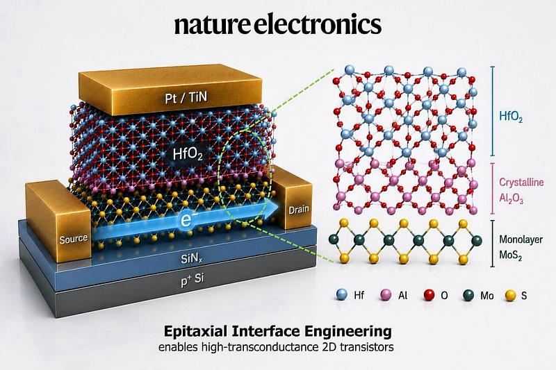
Researchers at Taiwan's NYCU oxidised a 0.3-nanometre aluminium film into a 0.42-nanometre buffer that lets a very thin gate insulator form on molybdenum disulfide without leaking, and the flow they used still needs scaling.
The Product Desk · Product desk
What happened
- Researchers at Taiwan's NYCU deposited about 0.3 nanometres of aluminium onto an atomically thin molybdenum disulfide sheet, then oxidised it into a continuous aluminium oxide layer roughly 0.42 nanometres thick.
- MoS2 surfaces lack the dangling chemical bonds conventional insulators rely on, so those insulators can leave gaps that leak current and defects that scatter electrons in the channel below.
- The transistors they built had a gate dielectric with electrical control equivalent to roughly one nanometre of silicon dioxide while keeping leakage low and carrier transport strong.
- The process as run uses MoS2 transfer, ultrahigh-vacuum deposition and carefully controlled oxidation, and all three would need simplifying and scaling before commercial semiconductor production.
- The study appeared in Nature Electronics, and one of the researchers quoted on it, Tsung-En Lee, holds positions at both TSMC and NYCU.
Compiled by The Product DeskSomething wrong?How this is made
Why it matters
- capability A single MoS2 device now carries a very thin gate dielectric, strong electrostatic control and high mobility together, so the electrical argument for 2D channels can be made from one measurement.
- constraint The controlling variable is a 0.12-nanometre thickness gain during oxidation. Holding that constant across a wafer is a process-control problem, and it decides whether this recipe ever leaves a lab.
- decision For a group deciding where next year's money goes, the paper's case is that interface work on materials already in hand pays better than continuing the hunt for a new 2D semiconductor.
The step someone else has to reproduce is the oxidation. Aluminium goes down as a metal film and comes back as an oxide about 1.4 times as thick, a gain of 0.12 nanometres [17]. That gain has to come out the same everywhere on a wafer. The researchers describe their own version as a carefully controlled oxidation following an ultrahigh-vacuum deposition [9].
The buffer exists because molybdenum disulfide is an awkward surface to build on. Its surface lacks the dangling chemical bonds that conventional insulators need, so those insulators struggle to form a smooth, continuous layer on it [4]. The defects left behind cause two problems: current leaks through them, and they scatter electrons moving in the channel underneath, which cuts carrier mobility [5]. "Making the insulator thinner was only part of the challenge," said Professor Wen-Hao Chang of NYCU, the study's corresponding author [10]. "We also needed to safeguard the atomically thin semiconductor beneath," he said [11]. The aluminium oxide gives the main dielectric something uniform to form on, and it also keeps electrical disturbance from that dielectric away from the channel [6].
Gate control gets stronger the closer the gate sits to the channel, so the insulator keeps being pushed toward a few atoms thick [15]. The authors say their result addresses a three-way trade-off in 2D electronics: an extremely thin gate dielectric, strong electrostatic control and high electron mobility in the same device [8]. Interesting Engineering's write-up left out which main dielectric was used and how many devices were measured [18].
This one is for the gate-stack engineers. Anyone choosing a channel material for a product this year can skip it. When the next 2D-transistor result comes through, two things are worth checking: which of the three legs were measured on one device, and which steps of the flow a fab could run tomorrow. The NYCU group has the first [7]. By its own account, all three of its process steps still need simplifying and scaling before a fab could run them [9].
"When transistor components are just a few atomic layers thick, the interface becomes an integral part of the device, not just a boundary," said Professor Tsung-En Lee of TSMC and NYCU [12].
What to watch
- A version of the buffer formed on MoS2 grown directly on the wafer would remove the step furthest from a production line.
- Leakage and mobility spreads across many devices, instead of one equivalent-thickness figure, would show whether the oxidation window is manufacturable.
- Whether the ultrahigh-vacuum aluminium deposition is replaced by a step existing fab tools already run.