Build1 distinct publisher3 min readPublished
Logic vendors have made copper-to-copper bonding routine. Memory has not, because HBM has to place pre-tested dies one at a time. A relaxed stack-height rule let HBM4 skip the switch entirely.
The Engineer · Build desk

Compiled by The EngineerSomething wrong?How this is made
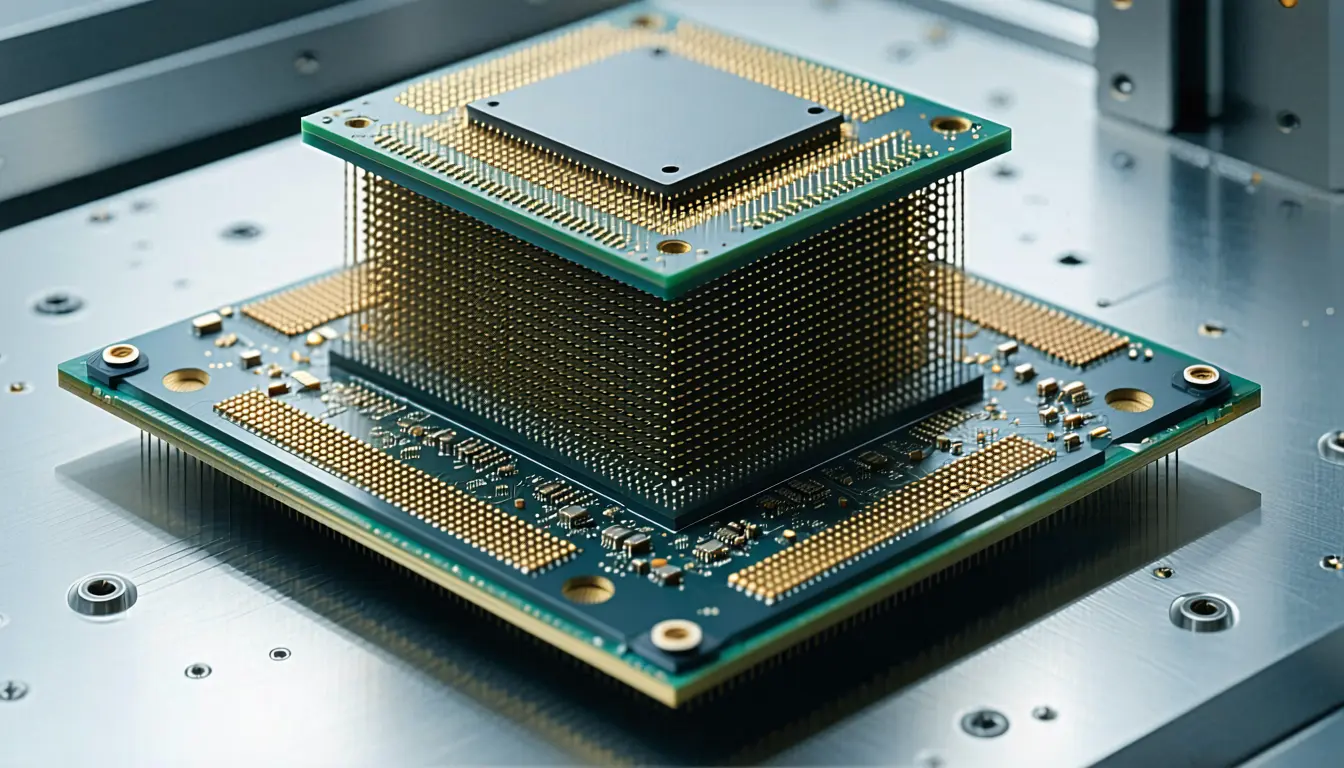
The split that decides all of this is wafer-to-wafer versus die-to-wafer. Wafer-to-wafer joins two full patterned wafers face to face and dices them afterwards, so alignment happens once at wafer scale [12]. That is where the tight numbers come from: imec and EV Group showed a 200-nanometre pitch with post-bond overlay under 40 nanometres at ECTC in May [14]. The price is that both wafers must carry identically sized dies, and every die gets bonded whether it tested good or not, so a single bad die ruins its partner [13].
An HBM stack cannot pay that. Memory needs pre-tested dies and the freedom to mix die sizes and process nodes, which means die-to-wafer [15]. The best die-to-wafer pitch at ECTC 2026 was CEA-Leti's 1 micron, roughly five times looser than the wafer-to-wafer record [17]. And because dies go down one at a time [16], the bonder sets the ceiling: Applied Materials and Besi cite around 1,600 placements per hour on the Kinex platform, and Besi's Chameo is rated near 2,000 chips per hour [18]. At 1,600 per hour, that is one placement every 2.25 seconds [23]. Multiply by the die count in a high stack and hybrid-bonded memory becomes a capacity question before it is a pitch question.
The height budget is why the rule change bites. Microbumps have only tightened toward 10 microns for the latest memory [10], while hybrid bonding starts at 6 and has 4.5- and 3-micron generations in development [11]. A taller stack allowance is exactly what lets a pitch that loose survive another product generation.
On the logic side, read the density figures for what they compare. The symposium ratio works out at 9.3 times [22], and it is a comparison of two topologies, not two pitches. Second-generation SoIC is what adds face-to-face bonding on top of the face-to-back stacking the first generation supported [3], so the higher number belongs to a pair of dies joined active surface to active surface. If your part is a tower rather than a pair, the face-to-back column is yours. AMD, which has used the technique in volume since the first 3D V-Cache parts [5], cites roughly 15 times the interconnect density of conventional 2.5D microbump stacking [8], which is a third baseline again.
The pitch roadmap deserves the same arithmetic. Moving from 6 microns to 4.5 by 2029 [2] is a 1.78x gain in pads per unit area [24]. That is a real gain, but it falls short of a doubling.
The surface spec is the part worth sitting with, more than the roadmap numbers. There is no solder bump: the copper pads and the surrounding dielectric bond directly under heat and pressure [7]. The dielectric grabs on contact through van der Waals forces, so the polished surface can vary by no more than about 0.2 nanometres, with the copper pads sitting a few nanometres below it and swelling into contact when the stack is heated to 200 to 300 C [19]. One particle under a micron across holds the two faces apart and opens a gap spanning many pads at once [20]. The tool that decides your yield is the polisher, and the hardest part of copper-to-copper bonding happens before any copper touches.
Ranked by verification strength, evidence, and original report placement.
Hybrid bonding, the copper-to-copper joining technique that replaces solder microbumps in 3D chip stacks, is in high-volume production on logic chips and has just been postponed for use with memory.
TSMC has scaled its SoIC bond pitch from 9 microns in 2023 to 6 microns in 2025, with a roadmap to 4.5 microns by 2029.
Second-generation TSMC SoIC adds face-to-face bonding on top of the face-to-back stacking that the first generation supported.
Intel began shipping Foveros Direct hybrid bonding in its Clearwater Forest server CPU in the first half of 2026.
AMD has used hybrid bonding in volume since the first 3D V-Cache parts.
A JEDEC decision earlier this year to raise the HBM stack-height limit lets HBM4 stay on microbump technology, deferring hybrid bonding in high-bandwidth memory to HBM4E and HBM5 at the end of the decade.
Distinct publishers with included, body-backed reporting in this cluster.
Follow any of these and your For You feed starts watching them — no settings page required.
build
SK hynix rules hybrid bonding out of HBM4E, leaving 55 microns to do the work1 distinct publisher
build
Glass-core substrates spent a billion dollars to arrive at package-level reliability evaluation1 distinct publisher
build
Micron's own numbers say the DRAM squeeze is an allocation problem, not a cycle1 distinct publisher
build
Samsung puts MAC trees in every LPDDR5X bank because HBM costs too much1 distinct publisher
Evidence-backed comparisons of source perspectives and observed adoption signals. Read the methodology
Which Builder, Operator, and Investor concerns the observed source mix emphasized—not a truth score.
Evidence, demonstrated adoption, hype gap, incentives, and confidence are assessed independently, each on its own current evidence. How these are measured.
One outlet, conference slides underneath
The technical spine is unusually specific for a single-source story: named pitches, named conference results, named tools. But every one of those numbers reaches the reader through Tom's Hardware relaying a symposium or ECTC presentation, and the claim the headline rests on, JEDEC's stack-height change, appears without a standards document, a date beyond "earlier this year", or a second outlet confirming it.
Shipping in logic, waiting in memory
This is not a laboratory technique looking for a customer. Intel ships it in a Xeon server part, AMD has shipped it since the first 3D V-Cache, TSMC runs it at 6 microns with Broadcom's Fujitsu Monaka and AMD's MI300 as reference designs, and two tool vendors quote production placement rates. The score stops short of the top because the largest volume application, HBM, has just voted to wait.
Density multipliers outrun the arithmetic
The framing is refreshingly deflationary, a story about a technology being told to wait. The overshoot is in the density figures: AMD's roughly 15 times sits next to TSMC symposium numbers that work out to about 9.3 times, the two are measuring different baselines, and neither is reconciled. Add that the piece calls the HBM delay one "nobody expected" while never establishing who expected otherwise.
Numbers supplied by the sellers
Follow the provenance of each figure and you arrive at someone with capacity or tooling to sell. The pitch roadmap is TSMC's own symposium material, the density multiple is AMD's, the placement rates come from Applied Materials and Besi describing their own bonders, and the capacity estimate is a research firm's. Only imec, EV Group and CEA-Leti are speaking from a consortium platform, and their records are the ones furthest from production.
Detailed but unchecked
Internally the account is coherent, and the causal argument holds up: known-good-die selection forces sequential placement, sequential placement caps throughput, so memory has a reason to stay on microbumps that logic does not. What keeps confidence middling is structural rather than substantive. Everything rests on one publisher's reading of vendor presentations, and the piece's own numbers disagree about how much density hybrid bonding actually buys.