BuildNot yet confirmed elsewhere1 publisher3 min readPublished
Samsung puts MAC trees in every LPDDR5X bank because HBM costs too much
At Hot Chips 2026 Samsung detailed a validated LPDDR5X-PIM part claiming 614 GB/s of internal bandwidth and 2.28x to 3.01x inference gains over plain LPDDR5X.
The Engineer · Build desk
What happened
- Samsung detailed LPDDR5X-PIM at Hot Chips 2026, putting in-memory logic into the low-power DRAM standard for the first time.
- The company floated LPDDR5X-PIM as a concept alongside HBM-PIM in 2023; what it showed this time is a validated product.
- LPDDR5X-9600 peaks at 76.8 GB/s, and Samsung says PIM raises effective bandwidth eightfold to 614 GB/s by keeping the arithmetic local.
Why it matters
- capability Keeping the 561-ball array and working with conventional DRAM controllers means a customer can evaluate PIM without redesigning the memory subsystem around it.
- decision SoC teams now have to decide whether to architect for in-memory MACs or wait for a JEDEC spec that would let them do it without single-sourcing from Samsung.
- precedent Fitting PIM into every bank without deleting banks removes the capacity penalty that made HBM-PIM a hard sell, which makes the same trick likelier in the next generations of commodity DRAM.
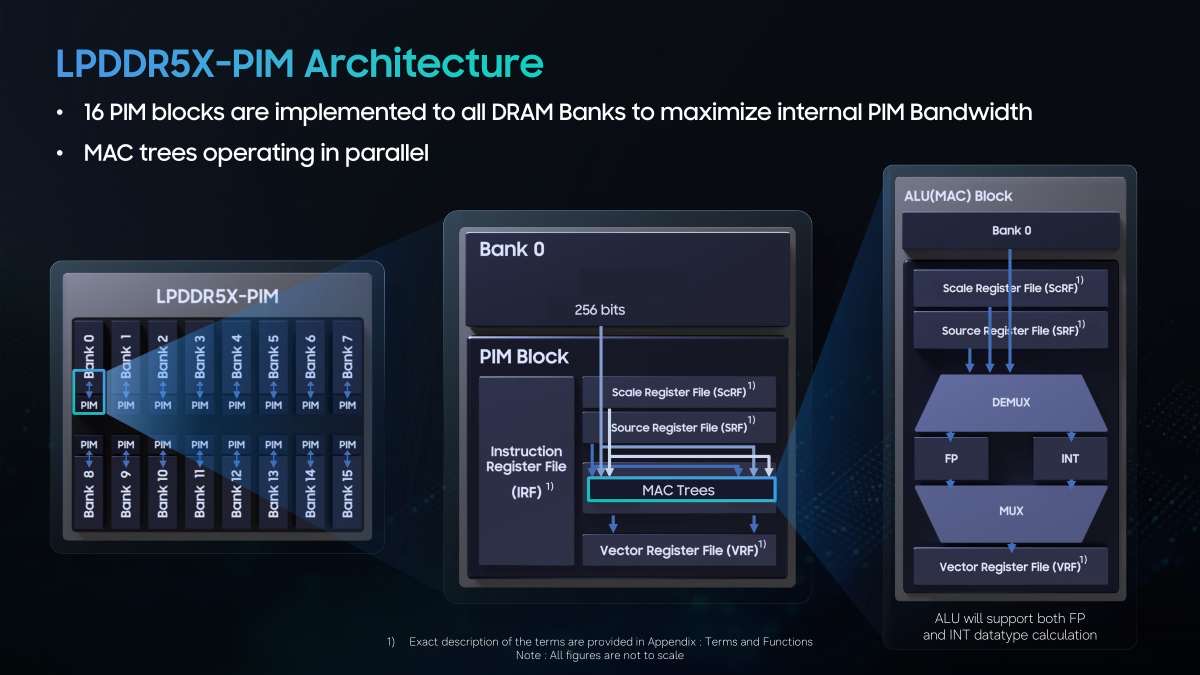
The interesting engineering is not the multiply-accumulate logic, which Samsung has been demonstrating since 2021 and shipped through HBM stacks in AMD accelerators [5]. It is that this time the logic did not cost any banks. In HBM-PIM, Samsung had to remove memory banks to make room for the compute; in LPDDR5X-PIM every bank gets its own PIM unit [7]. A DRAM vendor that can add arithmetic without giving up capacity has a much easier conversation with a phone or automotive customer than one asking for a capacity trade.
The 8x bandwidth figure is an internal number and should be read as such. LPDDR5X-9600 peaks at 76.8 GB/s at the package pins, and Samsung's 614 GB/s is what the MAC trees see because the operands never leave the die [3]. Divide it out and the multiplier is 7.99x [17], which is roughly what you would expect from sixteen banks working in parallel on data that used to be serialised through a 128-bit bus. The end-to-end result is far smaller: 2.28x on model run time, 3.01x on tokens per second [1][2]. That gap between 8x internal bandwidth and 2.28x wall-clock is the whole story of PIM. Only the parts of inference that reduce to MACs against resident weights get accelerated, and everything else still runs at LPDDR5X speed.
The compatibility work is where this gets plausible as a product rather than a paper. The package keeps the standard 561-ball array, two 64-bit ranks, 16 GB modules, four dies per rank [8][9]. Conventional DRAM controllers still work, with the part switching between single-bank standard mode and multi-bank PIM mode on the command stream [10]. Samsung's stated obstacle was command reordering in conventional DRAM, and its answer, Address Align Mode, derives the register file addresses from the row and column address instead of an instruction register file [11]. In other words, the reorder buffer can shuffle PIM commands and the operands still land in the right registers. That is the difference between needing a bespoke memory controller and needing a driver.
The constraints are visible in Samsung's own walkthrough. A 512-byte FP8 activation is split into sixteen 256-bit packets, one per bank [12]; the 1 kbit vector register file holds at most four results before it must be drained [13]; and getting the answer back means the host flipping to conventional mode and issuing sixteen reads [14]. Small working set, shallow accumulation depth, frequent mode changes. This is a design for batch-one inference on a device where the weights are already sitting in memory, not for anything resembling a training rack.
That is the part worth sitting with, because Samsung led its presentation with the cost argument: memory is the bulk of AI chip cost and rising, and Micron warned at the same event that HBM wafer demand is getting worse [6]. The response on offer is not cheaper HBM. It is arithmetic bolted to the cheapest, lowest-power DRAM in volume production, sold on the premise that a 2.28x speedup in a phone-class part is worth more than a fraction of an HBM stack nobody can buy. Samsung is already pointing at LPDDR6X-PIM and says it hopes for an initial JEDEC specification this year [15], which matters more than the benchmark: a standard would let SoC vendors design against PIM without betting on one supplier.
What to watch
- Whether JEDEC publishes an initial LPDDR6X-PIM specification this year, as Samsung says it hopes.
- Whether any named handset, automotive or edge customer commits to LPDDR5X-PIM silicon rather than evaluation parts.
- Whether the 2.28x and 3.01x figures survive third-party measurement on a stated model and quantisation.
Clarity's read
What the record supports and how the coverage leans. The claims behind it follow.
Reality
- Evidence52
- Adoption18
- Hype gap+34
- Incentives74
- Confidence55
Claim ledger
Ranked by verification strength, evidence, and original report placement.
- [1]
In Samsung's preliminary benchmarks, LPDDR5X-PIM showed a 2.28x improvement in model run time versus standard LPDDR5X.
- [2]
Samsung reports LPDDR5X-PIM is 3.01x faster than LPDDR5X in AI inference measured in tokens per second.
- [3]
With LPDDR5X-9600, peak bandwidth is 76.8 GB/s; with PIM this is increased eightfold to 614 GB/s by reducing data movement and keeping basic logic local.
- [4]
Samsung introduced the industry's first LPDDR5X-PIM memory, adding in-memory logic to the low-power memory standard, and detailed it at Hot Chips 2026.
- [5]
Processing-in-Memory is technology Samsung demoed as early as 2021 and piloted through HBM stacks in AMD accelerators; it is a small bit of logic beside DRAM cells allowing basic calculations to happen in memory.
- [6]
Samsung opened its Hot Chips presentation noting memory makes up the bulk of AI chip costs and its share continues to grow; Micron warned a day earlier at Hot Chips that HBM wafer demand is only getting worse.
- [7]
In LPDDR5X-PIM each memory bank has its own PIM unit, an advancement over HBM-PIM where Samsung had to cut banks to fit the logic.
- [8]
LPDDR5X-PIM uses a standard 561-ball array for packaging, just like LPDDR5X, with two 64-bit ranks and 16 GB modules.
- [10]
The part operates in two modes, single-bank (traditional DRAM) or multi-bank (PIM), and traditional DRAM controllers work, with commands switching between standard read/write and PIM read/write depending on mode.
- [11]
Samsung says the challenge was command reordering with conventional DRAM, and it uses Address Align Mode to map DRAM addresses to MAC instructions, assigning VRF/SRF addresses from the RA/CA address rather than the Instruction Register File.
- [12]
In Samsung's example, 512 bytes of FP8 activation data is broken into 16 256-bit packets written into each of the banks and noted in the Source Register File.
- [13]
With a VRF size of 1 kbit, a maximum of four calculations can be written to the Vector Register File.
- [14]
To collect results, the host switches to single-bank conventional DRAM mode and executes 16 reads to gather the output from all of the memory banks.
- [15]
Samsung is looking ahead to LPDDR6X-PIM and says it hopes to have an initial specification from JEDEC this year.
- [16]
Samsung introduced HBM-PIM in 2023 and at the time introduced the concept of LPDDR5X-PIM; what it shared at Hot Chips is a real product put through validation.
- [17]
614 GB/s divided by 76.8 GB/s is 7.99x.
Sources
1 independent publisher whose own reporting we read for this story.
Topics and entities
Follow any of these and your For You feed starts watching them — no settings page required.