BuildNot yet confirmed elsewhere1 publisher3 min readPublished
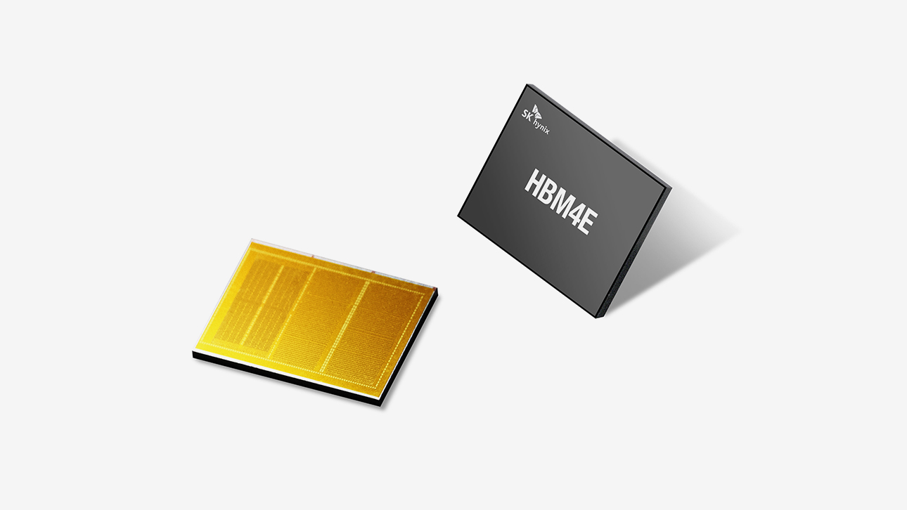
SK hynix rules hybrid bonding out of HBM4E, leaving 55 microns to do the work
Copper-to-copper slips to HBM5 at the earliest, so HBM4E capacity has to come out of die thickness inside a 775-micron package. iHBM heat blocks cannot be retrofitted to parts already in design.
The Engineer · Build desk
What happened
- SK hynix's package engineering VP told Hot Chips on August 23 that hybrid bonding will not be ready for HBM4E, putting the copper transition at HBM5 at the earliest.
- HBM cubes are capped at 775 microns total, the thickness of a 300mm logic wafer, so extra layers have to come out of die thickness and gap width.
- The cap exists because cold plate attach grinds both logic die and memory stacks back to bare silicon, and a taller cube would stand proud of the processor.
- 16-Hi HBM4 is in customer qualification at 48GB per cube, with 12-Hi already in mass production.
Why it matters
- constraint With copper bonding off the table through HBM4E, every added gigabyte has to be taken out of die and gap thickness inside a ceiling no single vendor can raise.
- decision Cooling becomes a calendar question rather than a purchase: a customer who wants iHBM has to wait for a generation whose design is still open, and skip the ones that are not.
- contradiction Samsung committed publicly to hybrid bonding for HBM4 last May; SK hynix now rules it out through HBM4E. The two are not describing the same crossover point.
- precedent Every previous JEDEC thickness raise bought MR-MUF one more generation, so the 20-Hi ceiling debate makes another reprieve the expected outcome rather than a surprise.
Run the arithmetic on the headroom JEDEC actually granted. The package ceiling went from 720 microns, which held through HBM3E, to 775 microns for HBM4 [7]. That is 55 microns [21] to absorb the step from 12-Hi to 16-Hi, or about 13.75 microns per added die [22], and each of those microns has to cover the die, the gap beneath it, and whatever fills the gap. Lee's own number for 16-Hi core dies, around 50 microns [5], does not close either: sixteen of them is 800 microns [23], past the ceiling before a base die or a single joint is counted. So the shipping core die sits under the round number in the deck, or the base and top dies give back the difference.
The heat side moves faster than the thickness side. Pin speeds have gone from 1 Gbps in early HBM to 8 Gbps in HBM4 [10], an eightfold rise into the same footprint, against a thermal burden SK hynix puts at 2.2 times across the generations shown [11][25]. The stack that has to carry that heat out is getting proportionally more oxide as dies thin, and oxide is a poor conductor next to silicon [9]. MR-MUF places every die by pick-and-place and joins them in one reflow [12], and Lee named the real difficulty of 16-Hi as filling gaps that have halved while keeping sub-50-micron dies flat [12][5].
Copper bonding would buy back room. Removing micro-bumps lets core dies grow up to 24% thicker at 20-Hi, cuts thermal resistance by roughly 35% against MR-MUF at that height, and takes bump pitch below 18 microns against 30 today [17], at least 40% finer [26]. It is also still a research item above 20 layers, with no product named yet [15]. "This is a very simple process, but in reality it's really challenging," Lee said of stacking 16 and 20 layers that way [20]. None of it is urgent while the ceiling keeps moving: industry discussion of 825 to 900 microns for 20-Hi [28] would add another 50 to 125 microns of relief [30]. The hedge is priced to match, one inline system pairing Applied Materials and Besi tools at about 20 billion won, or $15 million, per industry sources in March [29]. Counterpoint Research expects full-scale hybrid bonding at HBM5 around 2029 to 2030 [14], three to four years past the Hot Chips talk [27].
The cooling story carries the harder commercial term. iHBM embeds thermally conductive, electrically insulating blocks in the base die's die-to-die PHY region, where power density peaks, for a claimed reduction in thermal resistance of more than 30% [1]. Lee's constraint is that the blocks cannot be applied to any HBM generation already in design [6]. That is a gate on the design calendar, not a lead time. And the comparison set is unaudited: Samsung's Heat Path Block routes heat through dedicated pillars, Micron redesigns the base-die circuit for a claimed 20%-plus energy efficiency gain, and all three are vendor figures from vendor benchmarks [19]. Anyone specifying HBM4E now has the packaging answer already: mass reflow, 775 microns, no heat blocks.
What to watch
- Whether JEDEC actually relaxes the package ceiling to 825 to 900 microns for 20-Hi, which would delay the copper crossover again.
- Whether SK hynix names the first hybrid bonding product, and whether the single Applied Materials and Besi inline system grows into volume capacity.
- Which HBM generation is still early enough in design to accept iHBM blocks, and whether any customer commits to it.
Clarity's read
What the record supports and how the coverage leans. The claims behind it follow.
Reality
- Evidence61
- Adoption44
- Hype gap+9
- Incentives73
- Confidence56
Claim ledger
Ranked by verification strength, evidence, and original report placement.
- [1]
The iHBM concept, unveiled in May and detailed again three months later, embeds thermally conductive, electrically insulating blocks into the base die's die-to-die PHY region, the interface hotspot where power density peaks, for a claimed thermal resistance reduction of more than 30%.
- [2]
Jaesik Lee, VP of package engineering at SK hynix America, said during a presentation at Hot Chips 2026 on August 23 that SK hynix does not expect hybrid bonding to be ready for HBM4E, pushing the transition to HBM5 at the earliest.
- [3]
HBM cubes are capped at a total thickness of 775 microns, the standard thickness of a 300mm logic wafer, so every additional DRAM layer must come from thinner dies and narrower gaps.
- [4]
16-Hi HBM4 is in customer qualification at 48GB per cube, while 12-Hi is in mass production.
- [5]
16-Hi HBM4 thins its core dies to around 50 microns and halves the gap between them compared with 12-Hi.
- [6]
Lee said the iHBM heat blocks cannot be applied to any HBM generation already in design.
- [7]
The JEDEC HBM4 standard raised the package thickness ceiling from 720 microns, which held through HBM3E, to 775 microns, easing the pressure to adopt hybrid bonding.
- [8]
When a GPU package gets its cold plate attached, both the logic die and the memory stacks are ground back to expose bare silicon, so a memory cube taller than the 775-micron logic wafer would stand proud of the processor beside it.
- [9]
Thinner dies leave the stack with proportionally more oxide, which conducts heat poorly compared with silicon.
- [10]
Pin speeds have risen from 1 Gbps in early HBM to 8 Gbps in HBM4, concentrating more power in the same footprint.
- [11]
SK hynix's own figures put the thermal burden at 2.2 times higher across the HBM generations shown, while stack counts double every two generations.
- [12]
SK hynix's mass reflow-molded underfill (MR-MUF) process stacks all dies via pick-and-place and joins them in a single reflow; per Lee, filling gaps that have shrunk by half while controlling warpage on sub-50-micron dies is the main manufacturing challenge of 16-Hi.
- [13]
Samsung publicly committed to hybrid bonding for HBM4 in May last year, while SK hynix held the copper-to-copper technique as a backup behind advanced MR-MUF.
- [14]
Counterpoint Research expects hybrid bonding to enter full-scale HBM production with HBM5 around 2029 to 2030.
- [15]
Per the presentation roadmap, hybrid bonding remains at the research stage for stacks of 20 layers and above, and SK hynix is still deciding which product gets it first.
- [16]
Hybrid bonding joins flattened copper pads and oxide surfaces at room temperature, then relies on copper's thermal expansion during a cure step to form the bond.
- [17]
Per the deck, removing micro-bumps entirely lets core dies grow up to 24% thicker at 20-Hi, cuts thermal resistance by roughly 35% versus MR-MUF at that height, and takes bump pitch below 18 microns against the 30 microns where MR-MUF is today.
- [18]
At HBM4's bump pitch, conventional micro-bumps still work, and each time JEDEC has raised the thickness ceiling, MR-MUF has stayed viable for another generation.
- [19]
Lee's slides benchmarked iHBM against Samsung's Heat Path Block approach, which routes heat out of the stack through dedicated pillars, and Micron's base-die circuit redesign, which claims over 20% better energy efficiency; all three are vendor claims.
- [20]
Lee said of hybrid bonding: "This is a very simple process, but in reality it's really challenging. We are talking about 16 layers and 20 layers that we need to make the hybrid bonding, so it's very different from the one-layer stacking."
- [21]
The JEDEC HBM4 relaxation added 55 microns of package thickness headroom.
- [22]
Spread across the four extra dies between 12-Hi and 16-Hi, the 55 microns of added headroom works out to about 13.75 microns per added layer, covering die, gap and gap fill.
- [23]
Sixteen core dies at 50 microns each would total 800 microns, above the 775-micron ceiling before any base die, gap or joint is counted.
- [24]
A 48GB 16-Hi cube averages 3GB per core die.
- [25]
Pin speed has risen eightfold from early HBM to HBM4 while SK hynix's stated thermal burden across the generations shown rose 2.2 times.
- [26]
Going below 18 microns of bump pitch from 30 microns is a reduction of at least 40%.
- [27]
Counterpoint's 2029 to 2030 window for full-scale hybrid bonding sits about three to four years after the August 2026 Hot Chips presentation.
- [28]
Industry discussions now weigh a further move to 825 to 900 microns for 20-Hi stacks, which would push the copper-bonding crossover out again.
- [29]
In March, industry sources claimed SK hynix placed its first mass-production hybrid bonding order, a single inline system pairing Applied Materials and Besi tools worth around 20 billion won ($15 million).
- [30]
A move to 825 to 900 microns would add 50 to 125 microns over the current 775-micron ceiling.
Sources
1 independent publisher whose own reporting we read for this story.
Topics and entities
Follow any of these and your For You feed starts watching them — no settings page required.
Topics
- Chip Thermal ManagementFollow
- JEDEC Memory StandardsFollow
- AI Accelerator Memory SystemsFollow
- High-Bandwidth MemoryFollow
- Advanced Chip PackagingFollow
- Hybrid BondingFollow
- Semiconductor EquipmentFollow
Entities
- SK hynixFollow
- Jaesik LeeFollow
- HBM4Follow
- HBM4EFollow
- HBM5Follow
- MR-MUFFollow
- Hybrid bondingFollow
- iHBMFollow
- JEDECFollow
- SamsungFollow
- MicronFollow
- Hot Chips 2026Follow
- Counterpoint ResearchFollow
- Applied MaterialsFollow
- BesiFollow
- NvidiaFollow
- Vera RubinFollow
- SanDiskFollow
- High-Bandwidth Flash (HBF)Follow
- SemiAnalysisFollow
- Tanj BennettFollow