Product2 publishers3 min readPublished Updated
SK Hynix dates its first US HBM packaging line to the second half of 2029
The Indiana plant broke ground in August with a clean room due by October 2028 and next-generation HBM in mass production the following year, which leaves anyone specifying memory for a 2027 product buying from today's lines.
The Product Desk · Product desk
What happened
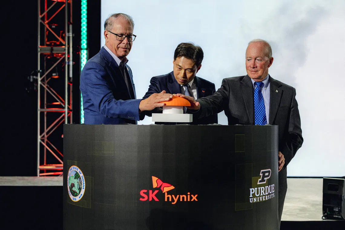
- SK Hynix broke ground on Aug 27 for its first US high-bandwidth memory packaging base, a 54-hectare site at West Lafayette, Indiana, that the company puts at more than US$4 billion.
- The project draws on the 2022 Chips and Science Act, which allowed SK Hynix as much as US$458 million in direct funding and up to US$500 million in loans.
- SK Hynix expects about 1,000 employees once the hub is fully operational and roughly 7,000 direct and indirect jobs once construction and related industry are counted.
Compiled by The Product DeskSomething wrong?How this is made
Why it matters
- constraint No part of this schedule reaches a bill of materials for a product shipping before the end of the decade, so memory in current planning remains a negotiation with lines that already run.
- decision Buyers weighing multi-year allocation contracts now have a firm date to anchor against, and it sits well past the product cycles being specified this year.
- exposure Sourcing HBM packaged in Indiana will not reduce a customer's exposure to a front-end outage in South Korea, so the dual-sourcing argument survives the ribbon cutting.
- cost Public money covers at most about a quarter of the build at the announced ceilings, which leaves the schedule and overrun risk sitting on SK Hynix's own balance sheet.
Anyone filling in a 2027 bill of materials this week with a placeholder where the memory price should go will likely see this groundbreaking forwarded from someone senior. The dates in it do not reach their product.
The two milestones sit close together. The clean room is expected to open by October 2028, and mass production begins in the second half of 2029, according to chief executive Kwak Noh-jung [3]. The earliest month of that half leaves a gap of about nine months to move tools in and qualify a line [16]. That is a normal ramp, and it is the only schedule buffer in the announcement. The other word doing quiet work is "next-generation" [3]: the parts coming off this line in 2029 are not the parts in a design being frozen now, so this capacity sits outside the HBM generation currently under allocation.
The second thing worth separating is what actually gets localised. SK Hynix says wafers produced in South Korea will be shipped to Indiana for packaging and testing before going to US customers [6]. Advanced packaging is the weak link the project targets, the step that stacks multiple dies into one package [10], and HBM is a prerequisite for assembling Nvidia's most advanced AI systems [8]. So a buyer in 2029 gets US packaging and test on Korean-fabbed wafers. Geographic risk on the front end stays where it is.
On the money, the CHIPS and Science Act allows as much as US$458 million in direct funding and up to US$500 million in loans [7], which is up to US$958 million of public support [13] against a build the company puts above US$4 billion [2]. At the ceilings, that is roughly 24 percent [14], and less if the cost climbs. Worth noting for anyone quoting the figure: the Straits Times headline says $5 billion while its own text says more than US$4 billion and gives S$5.08 billion, the Singapore-dollar conversion [17]. The item is labelled AI generated and credited to Bloomberg [18]. Kwak's own framing was that SK Hynix will "become the most trusted partner in shaping the future of AI in America" [19], which is a sentence about 2030s positioning rather than about your Q3 memory quote.
Two questions decide whether this plant matters to you: does your product ship before the second half of 2029, and does it use the current HBM generation or the one after it? Ships early on current-generation parts, and your supply comes from existing lines. Ships early on next-generation parts, and the Indiana line is not yet running to supply it. Ships late on current-generation, and the Indiana output is described as next-generation, so it does not apply either. Only the ships-late, next-generation-part box is touched at all, and even there the benefit is packaging location rather than more wafers.
None of this source says what memory prices will do. What it does give planners is a dated increment of US HBM packaging capacity, and the date is in the second half of 2029 [3], with about 1,000 people running it when full [4]. Treat everything before then as a negotiation with lines that already exist, and price the memory line in a 2027 BOM accordingly.
What to watch
- Whether SK Hynix names which HBM generation the 2029 line will package, which decides if any part number now in design benefits.
- Whether the October 2028 clean-room date holds, since the nine-month margin to mass production is the entire schedule buffer.
- Whether the US$458 million in direct funding and US$500 million in loans are disbursed at those ceilings, and against which milestones.