Invest1 publisher3 min readPublished
Intel puts the industry's first commercial High NA EUV scanner into calibration in Oregon
The 1.7x resolution gain ASML's EXE:5000 promises is a number Intel can point at; the 2.9x density that follows is that number squared, and neither one carries a price for the tool or a date for 14A production.
The Investor · Invest desk
What happened
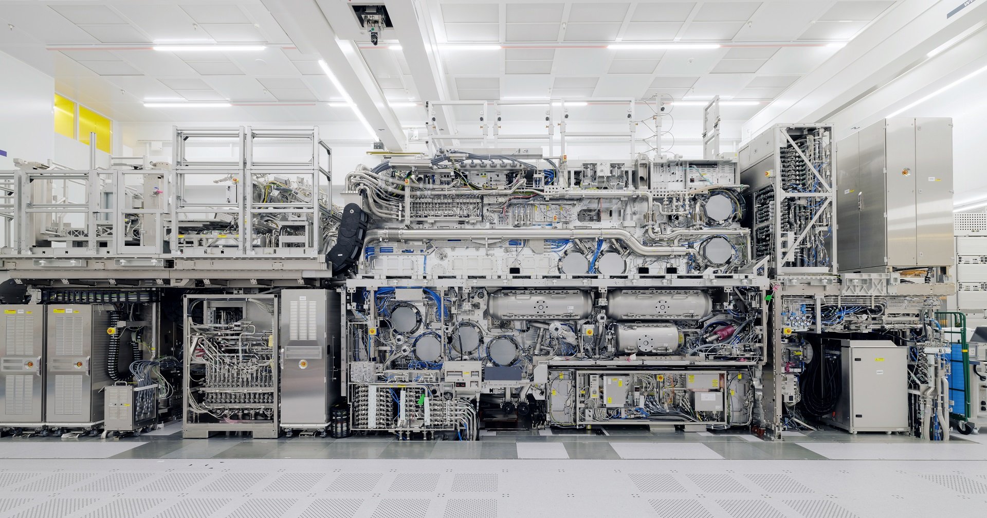
- Intel Foundry says assembly is complete on the industry's first commercial High NA EUV scanner, installed at the company's Hillsboro, Oregon research site.
- The tool, an ASML TWINSCAN EXE:5000, is now moving through calibration steps ahead of use in production of Intel's future process roadmap.
- ASML separately reported printing 10 nanometer dense lines at its Veldhoven lab, which it calls a world-record resolution for an EUV scanner and a validation of the Zeiss optics.
- Intel expects to run 0.33NA and 0.55NA tools alongside each other, with product proof points on Intel 18A in 2025 and use in production of Intel 14A.
Compiled by The InvestorSomething wrong?How this is made
Why it matters
- constraint Intel's only stated productivity number belongs to the EXE:5200B it has yet to acquire, leaving the tool now in Oregon without a public throughput figure to argue from.
- exposure Being first mover means Intel absorbs the calibration and debugging cost on a system no other buyer has taken into production, and any lessons learned arrive cheaper for whoever orders second.
- decision Because Intel intends to keep both numerical apertures in the flow, every layer becomes a make-or-buy choice between one High NA exposure and the established 0.33NA route.
Start with the arithmetic Intel's own release invites and then does not perform. High NA is expected to print features up to 1.7 times smaller than existing EUV tools, which enables two-dimensional scaling and up to 2.9 times more density [7]. The two figures describe a single optical improvement rather than two separate achievements: shrink a feature by 1.7 in each of two dimensions and you get 1.7 squared, or 2.89, which rounds to the density figure quoted alongside it [1]. The resolution number and the density number both trace back to that same claim.
What Intel has bought, on this evidence, is calendar. The company said it would adopt High NA in 2021 and reaffirmed the ASML collaboration in 2022 [11], and the release schedules product proof points on Intel 18A in 2025 with continuation into Intel 14A production [9], so the interval from procurement decision to first product proof point is four years [2]. That is the number a rival has to compress, and Intel's position is physical: more than 250 crates in 43 freight containers, flown into Seattle, trucked to Hillsboro, over 150 metric tons per system [10]. Repositioning a system that size takes years, not a quarterly reforecast.
The throughput case is where the money is, and it is where the release goes quiet. Higher imaging contrast at 0.55NA means less light per exposure, which cuts the time to print each layer and lifts wafer output [8]. Intel gives a productivity figure of more than 200 wafers per hour, but for the next-generation EXE:5200B it plans to acquire, not for the EXE:5000 now in calibration [12]; at that rate a single tool exposes one layer on 4,800 wafers a day if run flat out [3], though that number belongs to the future tool rather than the one now in Oregon, and neither machine has a published cost per wafer.
The interpretation depends on cost rather than physics, and it splits three ways. If 14A ships with High NA layers and the exposure-time gain shows up in wafer cost, then possession translates into a lead measured in tool-years. If High NA prints beautifully but never beats the 0.33NA path economically on the layers that matter, Intel ends up doing what it already says it will do, running both numerical apertures side by side [9], and first-mover status means Intel pays the tuition for everyone else who buys second. If 14A slips, the asset is an option on a node with no disclosed customers in this account.
The reading the evidence supports is the narrow one: Intel is first to physical possession and first to the calibration problem, and the record print ASML reported at Veldhoven, 10nm dense lines, came after coarse calibration of optics, sensors and stages rather than at full specification [5][6]. Full specification is still ahead of both companies. What would break the thesis that this is a durable advantage is a competitor disclosing a High NA order with a shorter path to production than four years, or a 14A cost per wafer that the mixed 0.33NA fleet already matches. Intel's release specifies the tin droplet temperature to the nearest thousand degrees, almost 220,000 Celsius [13], but never specifies the economics of the layer.
What to watch
- A dated 14A production start that names which layers are printed at 0.55NA, which is what turns calendar position into cost per wafer.
- Where the EXE:5200B Intel plans to acquire is installed, and whether it goes to an R&D site or a production fab.
- Any competitor disclosing a High NA order, and how much shorter its path from order to production is.