Product1 publisher3 min readPublished
Berkeley Lab imaged electron crystals melting around defects in MoSe2
A scanning tunneling microscope caught electrons inside molybdenum diselenide freezing into a crystal and melting into liquid-like waves, with the defect count in each sample deciding which state held. Quantum Monte Carlo simulations matched the images.
The Product Desk · Product desk
What happened
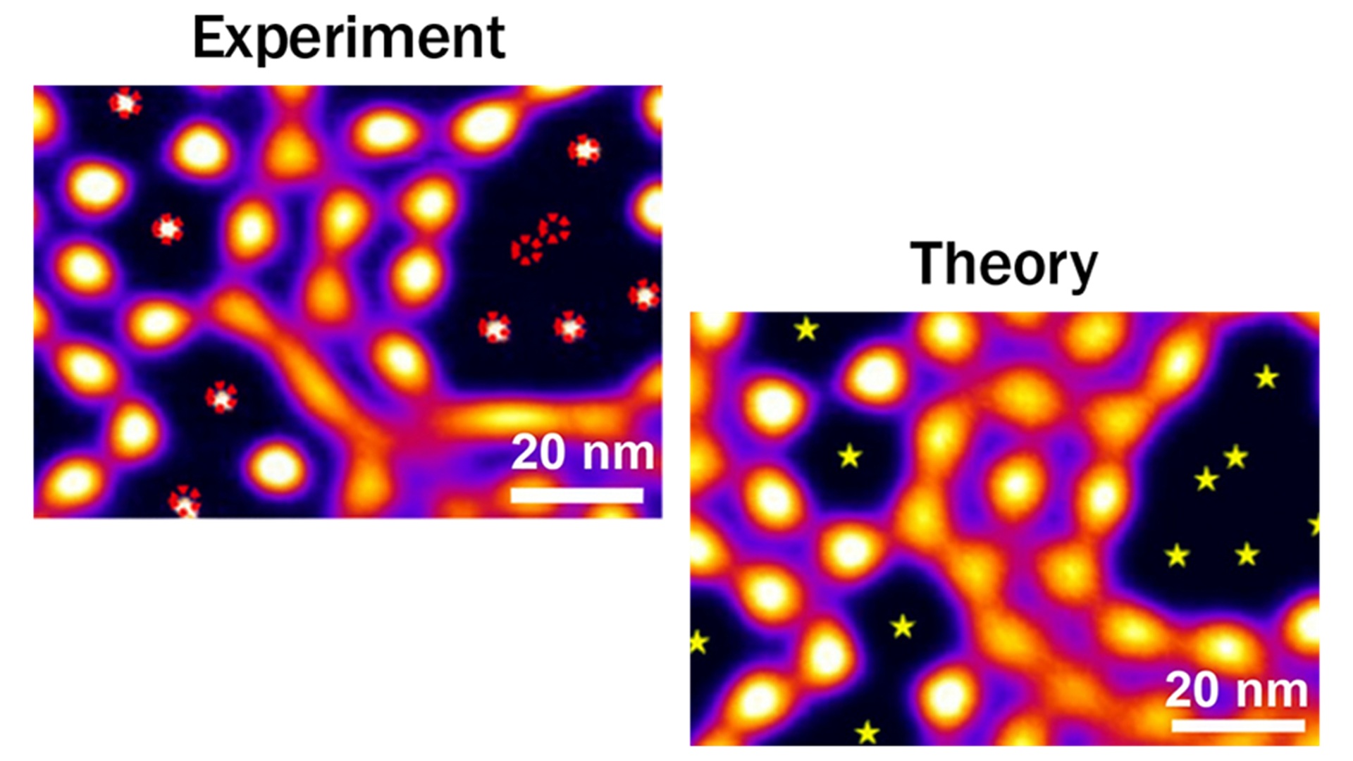
- A Berkeley Lab team used a scanning tunneling microscope to image both the electrons and the defects inside a semiconductor made from molybdenum diselenide.
- In samples with fewer defects, the electrons formed more orderly triangular, crystal-like patterns that transitioned more readily into the Fermi liquid state.
- To confirm the structures were genuine electron behavior and not microscope artifacts, the team ran Quantum Monte Carlo simulations, which closely matched what the images showed.
Compiled by The Product DeskSomething wrong?How this is made
Why it matters
- capability Defect-by-defect observation of strongly interacting electrons had been out of reach, so anyone arguing about defect engineering in 2D channels can now check the argument against images.
- decision Two wafers of the same 2D material are not interchangeable inputs, because the defect count decides which electron state the sample settles into. That puts sample screening ahead of material selection in the order of work.
- precedent Crommie's expectation that defect location and type will matter more as components shrink puts deliberate defect placement on the agenda for anyone designing a 2D channel, and someone will eventually have to specify it.
No process step changes this quarter because of a microscope image. According to Interesting Engineering's account of the work, direct observation of how defects act on strongly interacting electrons had not been managed before [8]. The Berkeley Lab group got the images, then checked them against Quantum Monte Carlo simulations of how quantum mechanics says those electrons should respond to random defects; the simulations closely matched the pictures [9]. The paper is in Nature [14].
What was actually done is narrow. One material, molybdenum diselenide [2], stacked between a graphite layer and layers of silicon and boron nitride, with tiny holes in the graphite so the microscope's metal tip could reach the semiconductor underneath [3]. Samples were sorted by defect level, and electron density was adjusted to drive the system between the two states [4]. MoSe2 sits in the class of 2D semiconductors, ultra-thin materials made from one or a few layers of atoms, and that thinness is what changes how electrons behave [20]. Mike Crommie, a Berkeley Lab scientist and UC Berkeley physics professor [16], put the broader claim this way: "Our methods open the door to the discovery of never-seen-before electron behaviors that can be used for new semiconductor capabilities" [11].
In a Wigner solid, free electrons freeze into a rigid crystal-like grid instead of flowing like a fluid; in a Fermi liquid they move more like independent particles [7]. The dirtier samples pinned the electron crystal into an unexpectedly stable Wigner solid, with irregular and disordered patterns [5]. Cleaner samples gave the tidy triangular lattice, and that lattice moved into the Fermi liquid state more readily [6]. Stability and order therefore ran in opposite directions with defect count [1]. Crommie described certain defects as acting like large potholes and others like tiny speed bumps [12]. On seeing the images he said: "It was exciting to see the Wigner solid melt into liquid-like waves splashing up against defects" [10].
The report does not state defect densities or the temperature at which the measurements were made [19]. The result describes samples, and a supplier would still be waiting on a number.
A claim like this has to get sorted when it arrives at a product decision. Whether the effect survives at the temperature and the dimensions the product runs at, and whether the defects can be put where you want them, on purpose, at volume. Yes to both and it is a process input. If only the second holds, it becomes a materials program with a target to hit. If only the first holds, it stays physics with no handle on it. This work answers neither question; it is the instrument that lets someone else answer the second. Crommie believes controlling the location and type of defects could become increasingly important as electronic components shrink [13].
What to watch
- Whether the Nature paper reports the temperatures and defect densities needed to reproduce the two sample regimes.
- Whether another group places defects deliberately, by position and type, and gets the electron state it predicted.
- Whether the holes-in-a-graphite-gate imaging trick gets applied to other 2D semiconductors.