Science1 publisher2 min readPublished
Berkeley Lab caught electrons and the defects that pin them in a single image
A Berkeley Lab-led group spent years building a molybdenum diselenide device that a scanning tunneling microscope could read, and it says the defects in that device are what hold the electrons in place.
The Scientist · Science desk
What happened
- A Berkeley Lab-led team reports in Nature that it directly observed how electrons interact with defects inside advanced semiconductor devices, alongside a new simulation tool for interpreting what it saw.
- The lab states the finding as defects locking electrons into stable Wigner solids, and calls the influence of those defects on electron behavior outsized.
- A Wigner solid is the state in which electrons stop moving and settle into a relatively orderly pattern because their mutual repulsion, not their independent motion, dominates their behavior.
- Earlier work on electron-defect interactions went through wires instead, measuring how easily electricity flowed through a device and reasoning backwards to the cause.
Compiled by The ScientistSomething wrong?How this is made
Why it matters
- capability Arguments about what holds electrons in place in a strongly interacting 2D system can now be tested against an image of the same spot. That is a different kind of evidence from a device-wide conductivity number.
- constraint The result depends on one hand-built stack that took years to make imageable, so this will not become a fast screen for candidate 2D device materials.
- precedent If disorder helps stabilize the pattern, then work on these states has to specify which defects and where they sit, and cleanliness alone stops being the only variable that matters.
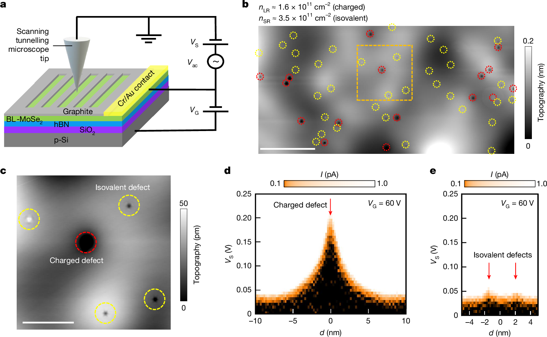
A scanning tunneling microscope hovers a tiny metal tip just above a material's surface and extracts current as the tip scans across [14]. Getting a working 2D semiconductor under that tip is the hard part. The team spent years on one sandwich: molybdenum diselenide between a graphite layer on top and a boron nitride layer and silicon wafer below, built for the highest structural and electronic resolution they could reach [15]. The difficulty of designing devices imageable at the scale of individual atoms is why, by Berkeley Lab's account, nobody had watched electrons and defects interact in a strongly interacting 2D system before [11].
A conductivity measurement returns one number for the whole device [12]. The tip returns a value at each position it visits [14]. "Some of the conclusions in these previous experiments were ambiguous because the researchers could not actually see the electrons and the defects at the same time," said Mike Crommie, a senior faculty scientist in Berkeley Lab's Materials Sciences Division and a professor of physics at UC Berkeley [13][5]. "They were inferring the behavior based on electrical conductivity," he said [13].
"Physicists call this conventional state a Fermi liquid because the electrons move around like waves in the ocean," Crommie said of the ordinary case, where electrons move as independent particles and their interactions with each other matter little to how a device works [9][8].
Berkeley Lab's account says electrons enter the Wigner solid state under certain conditions and leaves it there, without a defect density, a temperature or a carrier density [18][10]. Those numbers are what decide how far this carries. Imaging shows where electrons sit relative to defects in the patches the tip visited; how a wired device of the same material would conduct is a separate question.
The interest in these materials is that one layer, or a few, changes how electrons behave, where conventional chips are built from atoms arranged in three-dimensional structures [7]. Crommie put the payoff in the future tense. "Our methods open the door to the discovery of never-seen-before electron behaviors that can be used for new semiconductor capabilities. This will be important for the future development of semiconductor devices at the ultimate limits of miniaturization," he said [4]. Six institutions besides Berkeley Lab are named among the collaborators, including the Flatiron Institute and Japan's National Institute for Materials Science [17][6].
What to watch
- The Nature paper's numbers: the defect density, temperature and carrier density at which the pinning was seen, and whether pinning strength varies by defect type.
- Whether another group builds an equivalent scanning-tunneling-compatible 2D device stack. That is what would turn this from one experiment into a method.
- Whether transport measurements on these same devices agree with what the images show.