Product1 distinct publisher3 min readPublished
The diodes blocked 3.9 kV and held their on-resistance through repeated switching at 3 kV, but the transistor's switching losses were characterised only to 650 V, about a fifth of the voltage it blocks.
The Product Desk · Product desk

product
Canva's forecast cut turns model routing into a product line item1 distinct publisher
science
X-ray momentum maps finally make short-wavelength magnons measurable, and now theory is the slow part1 distinct publisher
build
A goal that writes itself into SOUL.md: agent memory is now an attack surface1 distinct publisher
security
A paragraph beat the agent "mind virus": reading the Anthropic-EPFL preprint as a defensive win1 distinct publisher
Compiled by The Product DeskSomething wrong?How this is made
Anyone who specifies power devices reads a datasheet in a fixed order: blocking voltage first, then the curves that say what the part costs every time it switches. The EPFL work is strong on the first reading and openly incomplete on the second, and the second is where a design gets decided.
The diodes did the heavy lifting. Schottky barrier diodes grown on a relatively inexpensive silicon substrate [5] broke down above 3.9 kV with specific on-resistance as low as 4.7 milliohm cm2 [6]. They stayed above 3.3 kV at 125 C [10], and their dynamic on-resistance rose by less than 15 percent under repeated operation up to 3 kV [11].
The transistors are the parts that would actually sit in a converter, and they were characterised less far. They sustained 3.5 kV normally-on and 3.4 kV normally-off [8], but dynamic on-resistance was measured only up to 650 V, because the team's setup introduced parasitic effects at higher switching voltages [12]. That covers roughly 19 percent of the normally-off blocking figure [15].
That 650 V has a second meaning. Interesting Engineering's account describes 3.4 kV as more than five times the rating of many commercial GaN power devices [9], which puts the implied baseline at 680 V or below [16], roughly the class GaN already sells into. So the switching behaviour of this transistor has been shown at the top of the voltage range GaN already serves, and the blocking behaviour five times above it. The two kilovolt figures describe different properties measured at very different voltages: blocking voltage and switching-loss voltage, and they should not be read as a single rating.
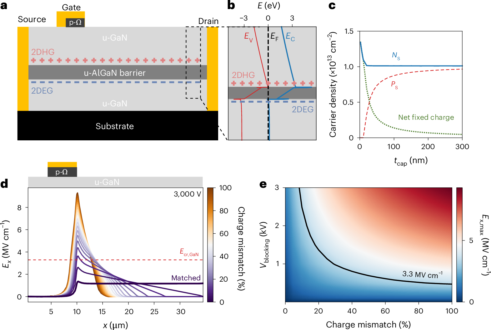
The mechanism earns its attention. GaN's spontaneous and piezoelectric polarization already yields a sheet of mobile electrons, and the team added a layer that produces a matching sheet of mobile holes, tuning the cap thickness until the two nearly cancelled: about 1.03 x 10^13 electrons per square centimetre against 1.05 x 10^13 holes [2][3], a mismatch near 1.9 percent [18]. A control device with mismatched sheets broke down below 1 kV where the balanced one reached 3.9 kV [7], a factor of at least 3.9 attributable to the match itself [17]. Because the balance comes from layer thickness rather than implanted dopants [4], it sidesteps what EPFL PhD student Yuan Zong calls the high temperature sensitivity of doping-based charge balancing in GaN [4].
For the person specifying parts, this stays a lab result rather than a catalog item. The account reports device-level measurements and gives no wafer size, yield, qualification status or availability [19]. What is usable is a two-column table per candidate device. Column one: the voltage at which off-state blocking was demonstrated, and the temperature it was demonstrated at. Column two: the voltage at which repeated switching loss was demonstrated, and its temperature. On this evidence, the diodes fill both columns out to about 3 kV; the transistor fills the first to 3.4 kV and the second to 650 V. Where column two is a fraction of column one, the loss line in the thermal model belongs to whoever builds the model, not to the device, and column two is the thing worth asking a supplier to date.
Ranked by verification strength, evidence, and original report placement.
Researchers at EPFL found a way to make GaN handle more than 3.4 kV by turning one of the material's natural properties into a built-in defence against electrical breakdown.
EPFL's POWERlab engineered an additional GaN layer that naturally creates a two-dimensional hole gas alongside the conventional two-dimensional electron gas, exploiting spontaneous and piezoelectric polarization; adjusting the thickness of the GaN cap layer let them tune the positive charge to match the negative charge.
In the devices, the 2DEG contained about 1.03 x 10^13 electrons per square centimetre and the 2DHG about 1.05 x 10^13 holes per square centimetre, a difference of less than 2 percent.
The approach removes the need for intentional doping to create the balancing charge. Yuan Zong, a lead researcher and PhD student at EPFL, said doping-based charge balancing in GaN can be highly temperature sensitive and that the doping-free design is key to the device's robustness.
The devices were built from layers of GaN on a relatively inexpensive silicon substrate.
The team demonstrated Schottky barrier diodes with breakdown voltages above 3.9 kV while maintaining a specific on-resistance as low as 4.7 milliohm cm2.
Distinct publishers with included, body-backed reporting in this cluster.
1 article · August 30, 2026
Follow any of these and your For You feed starts watching them — no settings page required.
Evidence-backed comparisons of source perspectives and observed adoption signals. Read the methodology
Which Builder, Operator, and Investor concerns the observed source mix emphasized—not a truth score.
Evidence, demonstrated adoption, hype gap, incentives, and confidence are assessed independently, each on its own current evidence. How these are measured.
Specific numbers, one account, no primary record
The measurements are unusually concrete for a single-outlet story — two sheet densities, a specific on-resistance, breakdown figures hot and cold, a named control device — and the arithmetic inside them is self-consistent. But all of it reaches us through Interesting Engineering's retelling of an EPFL study that is never identified by journal, title or date, and the three voices quoted all work in the same lab. The write-up's willingness to name its own weak spot, the 650 V switching test, is what keeps this above the midpoint rather than below it.
Nothing shipped to measure
There is simply nothing to count. These are bench devices: no wafer size, no yield, no qualification, no part number, no customer. The silicon substrate keeps a cost story plausible and the researchers' stated next step is combining this with their multi-channel work, which is a research roadmap rather than a product one. Assigning an adoption score here would be inventing one.
Headline runs past the 650 V test
The gap sits almost entirely in the framing rather than the data. '5x voltage leap for future EVs' rests on a commercial baseline nobody names, and on a transistor whose switching behaviour was measured across about a fifth of the voltage it blocks — the half of the promise operators care about most. Against that, the body text concedes the lab-only status and the substrate limit, and the diode results are not oversold. Overstated, then, but by the headline more than by the reporting under it.
Lab-sourced start to finish
Three quotes, one lab. Matioli, Zong and Mazzone all speak for POWERlab, and the closing paragraphs point readers toward the group's next project, which is how research communications are supposed to work and also how they shape a story. No funder, industrial partner, foundry or rival device maker is heard from, and the outlet's own pull toward a round '5x' number points the same direction as the institution's. None of this is concealed; it is just unbalanced by design.
Coherent, candid, uncorroborated
Two things pull against each other. The internal logic holds up: the densities reconcile with the stated mismatch, the control-versus-balanced ratio follows from the reported voltages, and the caveats are stated rather than buried. But one outlet, one lab and no traceable paper means a correction anywhere upstream would go unnoticed here, and the adoption picture is blank rather than weak. Enough to take the result seriously; not enough to lean on any single figure.