BuildNot yet confirmed elsewhere1 publisher3 min readPublished
Intel's Crescent Island bets 480GB of LPDDR5X and 350W beats paying for a liquid retrofit
Intel's Hot Chips disclosure details 32 Xe Cores, 32MB of L2 and 16-deep matrix engines. The figure it does not include is the one that decides whether the capacity is servable.
The Engineer · Build desk
What happened
- Intel used Hot Chips to detail the Xe3P architecture inside its Crescent Island AI accelerator.
- The part is a 350W air-cooled PCIe card with up to 480GB of LPDDR5X, aimed at conventional servers rather than liquid-cooled racks.
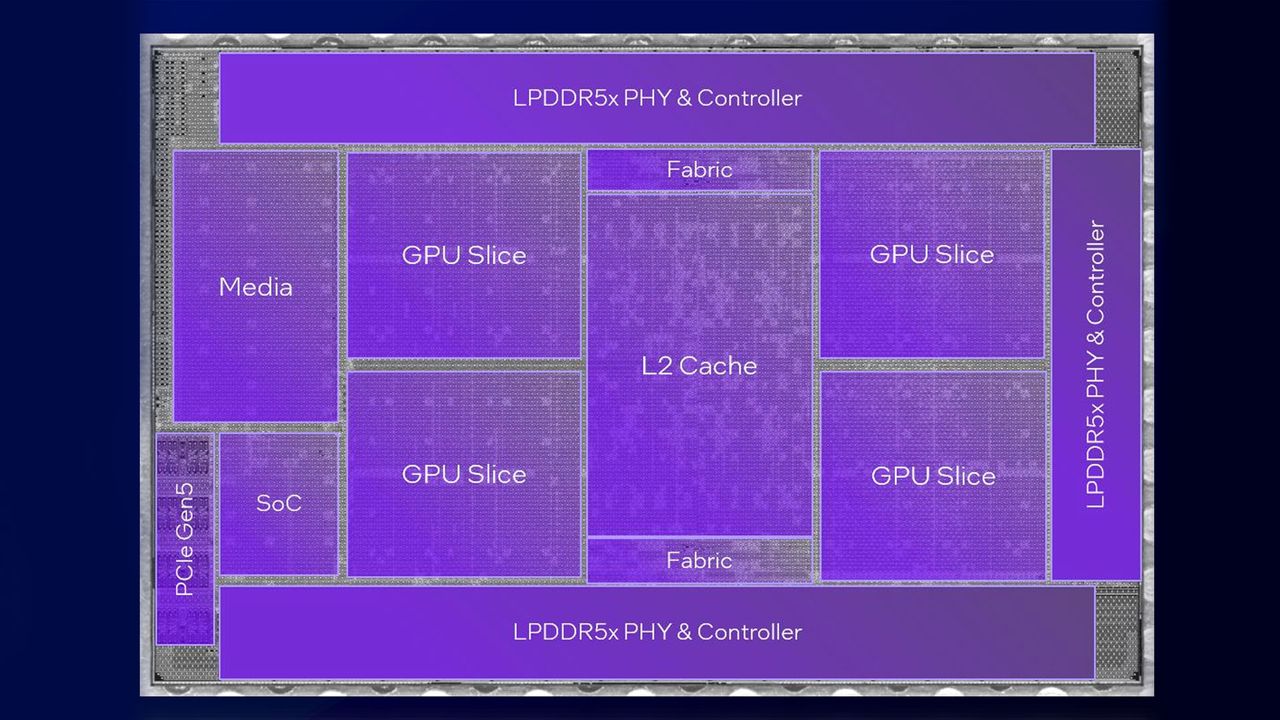
- Silicon is four Xe3P slices of eight Xe Cores, 32 in total, carrying 256 vector engines and 256 XMX matrix accelerators.
- Ray tracing hardware is gone to free die area for compute, though four media encoders and four decoders remain for multimodal input.
Why it matters
- constraint With no bandwidth figure disclosed, a buyer can size which models fit in 480GB but cannot model decode throughput, so the capacity claim cannot yet be turned into served tokens.
- decision Operators running air-cooled halls now have something to weigh against the capital cost of a liquid retrofit, rather than choosing between retrofitting and sitting out.
- exposure Intel's rationale depends on serving recipes staying compute-hungry; techniques that push decode back toward bandwidth-bound behaviour strand the design's advantage.
- capability Full-rate double precision lets one SKU chase converged HPC and AI tenders that would otherwise need separate hardware, which is why the FP64 units survived a die-area cut that killed ray tracing.
Add the per-core figures up and the design intent stops being a positioning statement. Thirty-two Xe Cores carrying 1MB of general register file each comes to 32MB of register space [12][3][19], the same amount as the shared L2 on the same die [4], with a further 16MB sitting in per-core L1 and shared local memory [5][20]. Intel says Xe3 already reworked the cache hierarchy to improve utilisation and cut register spills, and that Xe3P refines it further [2]. That is a large SRAM budget for an inference part, and it is the sort of budget you spend when the memory behind it is LPDDR5X rather than the HBM4 pools on Nvidia's Rubin and AMD's MI455X [1][11].
The matrix engines point the same way. Xe3P's XMX systolic arrays are 16 stages deep against four in Xe2 and Xe3, a fourfold increase [13][23], which on Intel's own description means each pass works through larger chunks of a matrix at once [13]. Deeper arrays and fatter register files buy the same thing: more arithmetic per byte pulled across the bus.
What the Hot Chips material does not contain, at least as reported by Tom's Hardware, is a memory bandwidth number [17]. Everything else is there in unusual detail, including a level of systolic-array description Tom's Hardware notes Nvidia does not offer for its Tensor Cores [24]. The workload Intel chose to highlight is the tell: mixture-of-experts models paired with speculative decoding [7], where a lightweight drafter proposes tokens the main model accepts or rejects, extracting useful work from compute that would otherwise idle [8]. Tom's Hardware notes that more aggressive drafting demands more compute [9]. Those are precisely the recipes that convert bandwidth-starved decode into batched matrix work. A part with plenty of resident capacity and deep XMX pipes is well matched to that regime and poorly matched to the one it replaced.
The FP64 decision is the other giveaway. Sixty-four FP64 FMA units per Xe Core is 2,048 across the die [12][6][21], full rate, on a chip Intel concedes is aimed at workloads where FP64 barely appears [6]. Ray tracing hardware was cut to preserve die area for compute [14], so the double-precision silicon survived a real trade. It is there to make the card biddable into converged HPC and AI procurements [6], alongside the ECC and parity coverage across the die that any data centre buyer will insist on [15].
Tom's Hardware frames the larger caches and deeper engines as a hunt for maximum AI FLOPS per watt [18]. The metric that actually follows from the parts list is different: 480GB inside a 350W envelope is roughly 1.37GB of resident model per watt [22], in a slot that needs no facility work [1]. For an operator with air-cooled halls, the comparison is not against Rubin's peak throughput but against the cost of plumbing a room that has no loop in it. Intel has built a card that only wins that comparison, and only if the bandwidth number, when it appears, is good enough to keep 480GB busy.
What to watch
- A published memory bandwidth figure for Crescent Island, and measured tokens per second on a named mixture-of-experts model at a stated batch size.
- OEM air-cooled server designs and per-GB pricing: capacity per slot only pays if the card is cheap enough per gigabyte resident.
- Whether serving stacks keep moving toward aggressive drafting, or back toward dense decode that puts pressure on memory bandwidth again.
Clarity's read
What the record supports and how the coverage leans. The claims behind it follow.
Reality
- Evidence58
- Adoption
- Insufficient
- Hype gap+30
- Incentives68
- Confidence52
Claim ledger
Ranked by verification strength, evidence, and original report placement.
- [1]
Crescent Island is a 350W air-cooled PCIe card using up to 480GB of LPDDR5X memory, so it can be deployed in traditional servers without exotic power and cooling requirements.
- [2]
The Xe3 architecture modified GPU cache hierarchy capacity and flexibility to improve utilisation and decrease register spills, and Xe3P further refines that hierarchy.
- [3]
Each Xe3P Xe Core has 1MB of general-purpose register file space, up from 512KB on Battlemage and Xe2.
- [4]
The chip has 32MB of shared L2 cache.
- [5]
Xe3P offers 512KB of L1 cache or shared local memory per Xe Core, a structure that began at 256KB on Battlemage and grew by roughly 1.33x on Panther Lake's Xe3 GPU.
- [6]
Crescent Island supports data types from MXFP4 up to what Intel describes as full-rate double precision, via 64 FP64 FMA units per Xe Core; Intel says FP64 is not widely used in AI workloads but its inclusion makes the chip useful as a converged HPC and AI part.
- [7]
Intel highlights the rise of mixture-of-experts models paired with speculative decoding as a new class of workload Crescent Island can serve well.
- [8]
Speculative decoding uses a fast, lightweight mechanism to draft future tokens that the main model then accepts or rejects, helping produce useful work from compute resources that would otherwise be idle.
- [9]
Tom's Hardware notes that as model serving recipes pursue more aggressive drafting mechanisms, more compute is required.
ReportedSupportedSource: Tom's Hardware2 sources— create a free account to open themView cited source - [10]
Intel shared more details of its Crescent Island AI accelerator, powered by the Xe3P architecture, at the Hot Chips symposium.
- [11]
Nvidia's Rubin and AMD's MI455X GPUs are high-power, exclusively liquid-cooled chips with massive pools of HBM4 memory that provide maximum performance across both AI training and inference; Crescent Island is instead designed to fit a lower-power, inference-first niche.
- [12]
Crescent Island is built from four Xe3P slices of eight Xe Cores each, 32 Xe Cores in total; each Xe Core has eight Xe Vector Engines and eight XMX matrix accelerators, for 256 of each.
- [13]
Xe3P's XMX systolic engines are a 16-deep design, versus the four-deep systolic design of Xe2 and Xe3, meaning they can process matrices in much larger chunks.
- [14]
Crescent Island has a media codec block with four encoders and four decoders for multimodal models, but graphics-specific functionality such as RT cores has been omitted to preserve die area for compute.
- [15]
As a data-centre part, Crescent Island offers a full suite of reliability, availability and serviceability features including ECC and parity protection across the die plus memory reliability features.
- [16]
Each Xe Core supports sigmoid and tanh transcendental functions, important to AI inference operations including softmax; AMD and Nvidia have also prioritised these functions in recent architectures.
- [17]
The Hot Chips disclosure as reported covers cache hierarchy, systolic depth, data types, media blocks and RAS features, but includes no memory bandwidth figure for Crescent Island.
- [18]
Tom's Hardware frames Crescent Island's larger caches and deeper XMX engines as targeting maximum AI FLOPS per watt.
- [19]
Aggregate general register file space across the die is 32MB, equal to the shared L2 capacity.
- [20]
Aggregate L1 cache and shared local memory across the die is 16MB.
- [21]
Crescent Island carries 2,048 FP64 FMA units in total.
- [22]
Crescent Island offers about 1.37GB of memory capacity per watt of board power.
- [23]
Xe3P's XMX systolic depth is four times that of Xe2 and Xe3.
- [24]
According to Tom's Hardware, Nvidia does not discuss the architecture of its Tensor Cores in anywhere near the level of detail Intel gave for Xe3P's systolic engines.
Sources
1 independent publisher whose own reporting we read for this story.
Topics and entities
Follow any of these and your For You feed starts watching them — no settings page required.