BuildNot yet confirmed elsewhere1 publisher3 min readPublished
Raptor's 0.37 pJ/bit is measured. The DRAM underneath it has no named fab.
d-Matrix says stacking compute on a co-designed DRAM die moves bits at roughly a sixth of HBM4's energy cost. It still has not said who fabricates the die.
The Engineer · Build desk
What happened
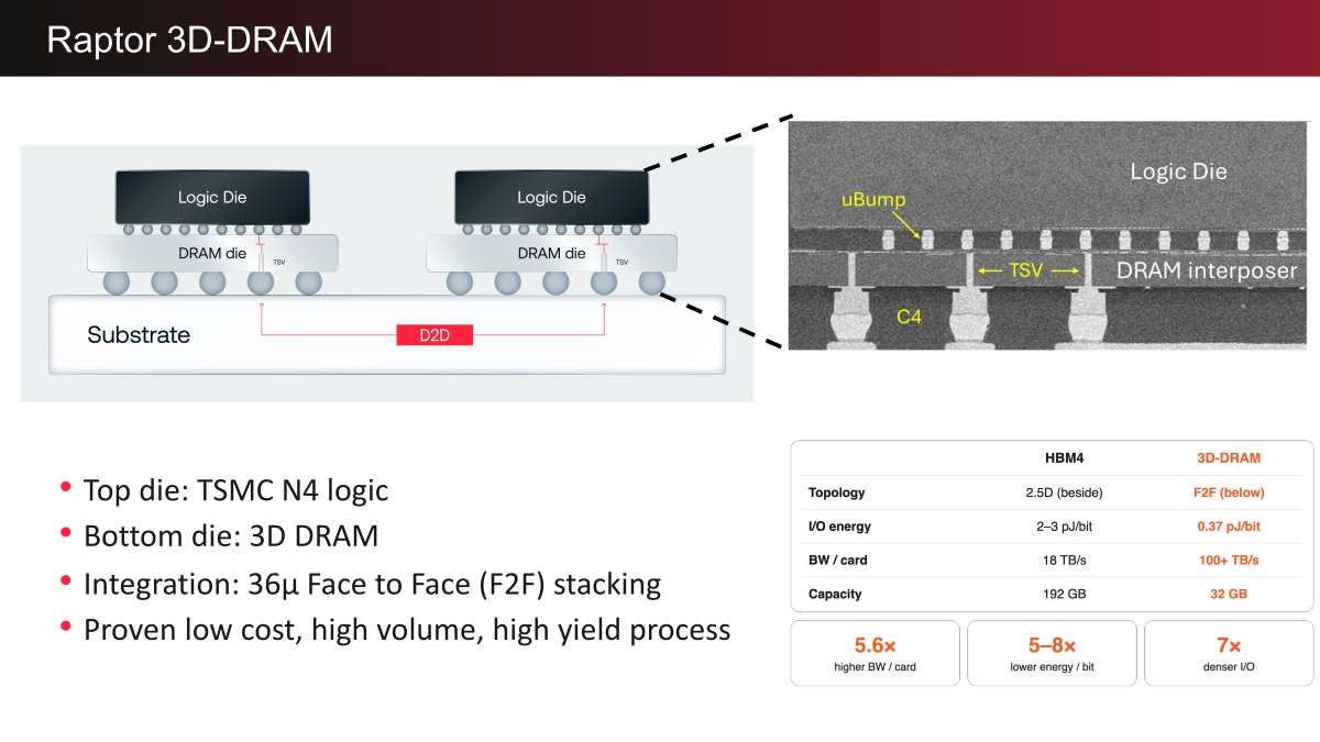
- d-Matrix showed Raptor at Hot Chips 2026: a TSMC 4nm compute die bonded face-to-face at 36-micron pitch onto a custom DRAM die, 100 TB/s from 32GB per card.
- The companion ISCA 2026 paper, co-written with the University of British Columbia, projects about 4.7 times the throughput per card of HBM-based designs.
- The company has still not said who fabricates the custom DRAM die, at Hot Chips or in any announcement since its Pavehawk test silicon last September.
- The CEO told CNBC in June that Raptor lands in 2027; at Hot Chips there was no date, no volume and no pricing.
Why it matters
- decision Anyone modelling 2027 inference cost per token off HBM energy and HBM availability now has a second column to fill in, with a claimed 6.5x gap in energy per bit moved sitting in it.
- constraint The efficiency cannot be bought as a part. It falls out of bank layout, refresh and ECC designed against one specific compute die, so a competitor cannot pick it up from a vendor catalogue.
- exposure A company that has raised about $450 million is asking one of three DRAM makers to give up HBM-grade wafer margin for a bespoke die, which leaves the 2027 schedule inside a supplier's discretion...
- contradiction One number is described as measured silicon and the rest, including the 4.7x throughput claim, are projections on early parts, so the energy argument and the performance argument carry very...
The 296W in the ISCA paper is the whole argument, and it is checkable. 100 TB/s is 800 terabits per second; multiply by 0.37 pJ/bit and you get 296W exactly [21]. So the disclosed interface power is the quoted efficiency running flat out, not a typical-case number with slack hidden in it. Push the same 800 Tb/s across an interface at the roughly 2.4 pJ/bit that CTO Sudeep Bhoja attributes to moving data into an HBM4 base die [1] and the data movement alone wants about 1.92kW [24], against a per-package budget of 422W [2]. Even at 0.37 pJ/bit, the vertical link is eating 70% of that budget [22].
That is why the stack is upside down. d-Matrix puts the logic die on top so a cold plate sits on the compute silicon, and the DRAM underneath doubles as the interposer, carrying PCIe and die-to-die signals down through its TSVs [8]. The bill for that arrangement is thermal: the DRAM is designed for a 105C junction, where retention falls from a standard 32ms to 4ms and refresh has to run eight times as often [9]. The fix is geometry, not cleverness in the controller. Each microbank was shrunk to 1,366 rows and about 5.33MB, so a full refresh sweep costs 1.37% of bandwidth [10].
The same pattern runs through the rest of the die. Yield is handled with 72 spare banks out of 840 per chiplet, wired into a two-level mux chain that swaps out any two failures while keeping channels symmetric [11]. Errors are caught by a [132,128] Reed-Solomon code on the logic die, two symbol errors per 128 bytes, with a CRC behind it [12]. There is no PHY, no burst structure and no sideband pins, which killed conventional data-bus inversion, so d-Matrix compares each 128-byte flit to the previous one and carries a 1-bit inversion tag next to the ECC metadata, recovering about 20% of the I/O power DBI would have saved [13].
Every one of those is a DRAM design decision. Which is the problem, because TSMC makes the N4P logic die and Alchip does the ASIC design and packaging, and neither runs a DRAM fab [14]. Three companies make leading-edge DRAM in volume, and their HBM4 lines are effectively sold out through 2026 [15]. Analysts logged DRAM contract price rises of 90% to 95% in Q1 2026 alone [16], and J.P. Morgan expects prices up more than 400% between the start of 2024 and the end of 2026 [17]. SK hynix CEO Kwak Noh-jung told Reuters in July that demand will exceed supply capacity even beyond 2030 [18]. Nvidia is reportedly testing Rubin Ultra with as little as 192GB because HBM4E may not be sourceable [25]. d-Matrix has raised about $450 million [19].
The energy figure is the least fragile thing on the table, and it is also the least transferable: it exists because the bank layout, refresh behaviour and interleaved ECC columns were designed against the compute die, and no memory vendor stocks anything resembling it [20]. That is a moat and a single point of failure in the same sentence.
What to watch
- Whether d-Matrix names a DRAM fabricator, or a second source, before it needs volume wafer starts for a 2027 launch.
- Whether 0.37 pJ/bit and the 4.7x throughput projection survive measurement on production cards at a 105C junction.
- Whether Nvidia's Rubin Ultra memory configurations shrink again, which would indicate how little slack the three DRAM makers have to sell anyone else.
Clarity's read
What the record supports and how the coverage leans. The claims behind it follow.
Reality
- Evidence58
- Adoption12
- Hype gap+32
- Incentives72
- Confidence55
Claim ledger
Ranked by verification strength, evidence, and original report placement.
- [1]
Co-founder and CTO Sudeep Bhoja put the vertical interface's energy cost at 0.37 pJ/bit against roughly 2.4 pJ/bit for moving data into an HBM4 base die, calling it "a measured number" from working silicon.
ReportedSupportedSource: d-Matrix CTO Sudeep Bhoja, via Tom's Hardware2 sources— create a free account to open themView cited source - [2]
At full tilt the vertical interface burns 296W of the 422W per-package budget the ISCA paper discloses.
- [3]
d-Matrix presented Raptor at Hot Chips 2026, calling it the first 3D DRAM accelerator for generative inference: a TSMC 4nm compute die bonded face-to-face at a 36-micron pitch on top of a custom DRAM die, delivering 100 TB/s of bandwidth from 32GB per card.
- [4]
The accompanying ISCA 2026 paper, written with the University of British Columbia, projects around 4.7 times higher throughput per card than HBM-based designs.
- [5]
Every performance figure shown at Hot Chips, including 988 tokens per second per user on the 2.8-trillion-parameter Kimi K3 model at 1M-token context, is a d-Matrix projection built on early silicon.
- [6]
Bhoja did not disclose who manufactures the DRAM die, and across the Hot Chips talk, the ISCA paper and every public announcement since the Pavehawk 3DIMC test silicon came online last September, d-Matrix has never identified who fabricates its custom DRAM.
- [7]
CEO Sid Sheth told CNBC in June that Raptor is slated to launch in 2027, but at Hot Chips the company gave no firm date and no information on volume or pricing.
- [8]
Raptor inverts the usual 3D stacking arrangement, putting the logic die on top and the DRAM underneath, so a cold plate sits directly on the compute silicon and the DRAM die doubles as the interposer, carrying PCIe and die-to-die signals down through its TSVs. The one-high stack reaches roughly 0.5W per square millimetre, which liquid cooling can handle.
- [9]
The DRAM is designed for a junction temperature of 105C, where retention collapses from a standard 32ms to 4ms and the memory must refresh eight times more often.
- [10]
d-Matrix absorbed the refresh penalty by shrinking each microbank to 1,366 rows and about 5.33MB, so a full refresh sweep costs only 1.37% of overall bandwidth.
- [11]
The die carries 840 banks per chiplet, of which 72 (around 9%) are spares wired into a two-level mux chain the company calls bank chaining, letting any two failed banks anywhere on the die be switched out while channels stay symmetric.
- [12]
A [132,128] Reed-Solomon code on the logic die corrects two symbol errors per 128 bytes, with a CRC behind it.
- [13]
The interface has no PHY, no burst structure and no sideband pins, so conventional data-bus inversion was impossible; d-Matrix instead compares each 128-byte flit to the previous one and stores a 1-bit inversion tag alongside the ECC metadata, recovering roughly 20% of the I/O power DBI would have saved.
- [14]
d-Matrix has named TSMC for the N4P logic die and Alchip as its ASIC design and 2.5D/3D packaging partner, but neither company operates a DRAM fab.
- [15]
Only three companies make leading-edge DRAM at volume, and all three are allocating capacity to HBM4 lines that are effectively sold out through 2026.
- [16]
Analysts have recorded DRAM contract price increases of 90% to 95% in Q1 2026 alone.
- [17]
J.P. Morgan estimates DRAM prices will have risen more than 400% between the start of 2024 and the end of 2026.
- [18]
SK hynix CEO Kwak Noh-jung told Reuters in July that "customer demand will remain higher than our supply capacity even beyond 2030."
- [20]
The bank geometry, spare-bank mux tree, refresh behaviour and interleaved ECC columns were all co-designed with the compute die; the 0.37 pJ/bit figure exists only because of that pairing, and no memory maker has anything like this die in its catalogue.
- [21]
100 TB/s at 0.37 pJ/bit works out to exactly 296W, matching the disclosed vertical-interface power, so the quoted efficiency is the figure at full bandwidth rather than a typical-case average.
- [22]
The vertical interface accounts for 70% of Raptor's disclosed 422W per-package power budget.
- [23]
0.37 pJ/bit against roughly 2.4 pJ/bit is about a 6.5-fold reduction in energy per bit moved.
- [24]
Moving 800 Tb/s at the roughly 2.4 pJ/bit d-Matrix attributes to an HBM4 base die would cost about 1,920W for data movement alone, roughly 4.5 times the whole 422W per-package budget.
- [25]
Nvidia is reportedly testing Rubin Ultra configurations with as little as 192GB because it may not be able to source enough HBM4E.
Sources
1 independent publisher whose own reporting we read for this story.
Topics and entities
Follow any of these and your For You feed starts watching them — no settings page required.