BuildNot yet confirmed elsewhere1 publisher3 min readPublished
Arm's AGI CPU finally has a spec sheet, and its best number needs DIMMs nobody sells yet
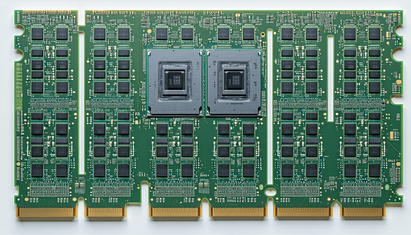
Two 70-core N3P chiplets, 12 DDR5 channels and a 2 TB/s UCIe link give capacity planners something to price. The 844.8 GB/s peak assumes DDR5-8800 modules Tom's Hardware says have not reached market.
The Engineer · Build desk
What happened
- Arm used Hot Chips 2026 to publish AGI's architecture and shipping configurations and to say the silicon works as planned, with commercial shipments starting late 2026.
- Each CSS V3 chiplet holds 70 Neoverse V3 cores and 50 billion transistors, with six DDR5 channels and a 2 TB/s UCIe link at 32 GT/s to its sibling.
- Configurations are 64, 128 or 136 cores clocked between 2.80 GHz and 3.70 GHz.
- Peak memory bandwidth is quoted at 844.8 GB/s with DDR5-8800 alongside a sub-100 ns latency claim, and that memory grade is not yet on the market.
- Compute and I/O sit together on each N3P die, unlike the split compute and I/O chiplets used by AMD, Intel and Nvidia.
Why it matters
- constraint The headline bandwidth depends on a memory grade nobody is shipping, so an AGI socket has to be modelled twice: once at DDR5-8800 and once at whatever speed grade a buyer can actually order.
- decision Racks being specified now face a live choice: hold slots for a 300 W, 136-core Arm socket arriving late 2026, or commit the whole refresh to x86.
- cost Keeping I/O on the same N3P die as the cores means the expensive node pays for both, with only four spare cores per socket standing between yield loss and a downgraded bin.
- contradiction The cache figures as published do not add up, which leaves per-core cache unresolved in exactly the comparison model a buyer needs.
On-die memory controllers are a latency purchase, and Arm paid for them in silicon. Each of the two AGI chiplets carries compute and I/O on the same N3P die [5], wired with an 8x9 CMN-S3 mesh, snoop filtering and a Super Home Node that distributes traffic through the chip [7], inside a coherency domain Arm built to reach past the die and the socket [8]. Memory traffic never crosses to a separate I/O die, which is how Arm arrives at a sub-100 ns DRAM latency claim [1]. Tom's Hardware reads the same floorplan as a trade: locality and bandwidth bought at the expense of the compute density, modularity and manufacturing ease that AMD gets from hanging compute chiplets off a central I/O die [11][13].
The numbers that matter to a purchase order are per core. Twelve DDR5 channels per socket, six on each chiplet [16], at DDR5-8800 gives 844.8 GB/s, and the arithmetic closes exactly at 12 x 8 bytes x 8800 MT/s [15][1]. Spread across 136 exposed cores that is 6.2 GB/s per core [18]. On the 64-core part, assuming it keeps both chiplets' controllers, the same bus serves 13.2 GB/s per core [19]. Against a 300 W socket [9], 136 cores works out to 2.2 W each [17].
That peak only exists if the DIMMs do. Tom's Hardware notes DDR5-8800 has still to reach the market [1], so anything quoted against an x86 bid this cycle carries a memory-speed contingency Arm does not control, and the fallback figure scales down with whatever grade is orderable in volume.
The cache disclosure does not reconcile. Arm's product-level number is up to 272 MB of system-level cache [6], but the per-chiplet detail is 128 MB of distributed SLC [7], which sums to 256 MB [24]. Meanwhile 272 is exactly 136 cores times 2 MB of L2 [23]. Either the top-line figure is aggregate L2 wearing a different label, or there is 16 MB of last-level cache Arm has not broken out. Cache per core is not a rounding error in a bid model.
Two 70-core chiplets is 140 physical cores and 100 billion transistors per socket [20][21] against a 136-core ceiling, so four cores of harvest slack [10]. The 64-core configuration exposes 46% of the physical cores [22], a wide bin for a part that still has to drive 96 lanes of PCIe 6.0 with CXL 3.0 on top [9].
Arm's original introduction gave key specifications and said nothing at all about performance [14]. Hot Chips added the architecture, the shipping configurations and a statement that the silicon works as planned [2]. That is enough to build a bandwidth and power model against, and not enough to build a throughput comparison, which is the first thing the x86 incumbents will put in front of a buyer.
What to watch
- DIMM vendors announcing DDR5-8800 availability, capacities and qualification: without them the 844.8 GB/s peak stays a paper number.
- Arm clarifying whether 272 MB is system-level cache or aggregate L2, and whether the 64-core part keeps all 12 memory channels.
- Any published AGI performance data, or named silicon and platform partners, before shipments start late 2026.
Clarity's read
What the record supports and how the coverage leans. The claims behind it follow.
Reality
- Evidence55
- Adoption8
- Hype gap+30
- Incentives65
- Confidence52
Claim ledger
Ranked by verification strength, evidence, and original report placement.
- [1]
Arm's design targets enormous memory bandwidth of 844.8 GB/s when used with DDR5-8800, though such memory still has to make it to the market, plus sub-100-ns DRAM latency.
- [2]
At Hot Chips 2026 Arm filled in architecture and design details of its AGI data center CPU, disclosed that the processor works as planned, published planned configurations, and said it is on track for commercial shipments in the coming months, with shipping starting late 2026.
- [3]
AGI is a dual-chiplet data center processor packing 64, 128 or 136 Neoverse V3 cores running at 2.80 GHz to 3.70 GHz.
- [4]
Each CSS V3 chiplet consists of 50 billion transistors, contains 70 Neoverse V3 cores and a six-channel memory subsystem supporting up to 3 TB of DDR5-8800 (6 TB per socket), and connects to its sibling using 16 x 16 UCIe macros at 32 GT/s for an aggregated 2 TB/s.
- [5]
Arm chose two largely self-contained SoC chiplets made on TSMC N3P, placing compute and I/O on the same die, rather than the heterogeneous multi-chiplet designs used by AMD, Intel and now Nvidia, all of which separate compute and I/O chiplets.
- [6]
AGI has two 128-bit vector engines and 2 MB of L2 cache per core, as well as up to 272 MB of system-level cache.
- [7]
Each chiplet uses an 8 x 9 CMN-S3 mesh to connect cores, memory, I/O and accelerators, and incorporates a 128 MB distributed system-level cache, snoop filtering and hierarchical caching through HN-S, or Super Home Node, which acts as a distribution center for traffic and data.
- [8]
CMN-S3 is not just an internal CPU mesh: Arm designed the coherent system to extend coherency beyond the die and the socket.
- [9]
AGI has 96 PCIe 6.0 lanes carrying the CXL 3.0 protocol for memory expansion, four PCIe 4.0 lanes, and I3C, I2C and SPI interfaces, with a thermal design power of 300 W.
- [10]
Each chiplet physically contains 70 Neoverse V3 cores but the complete product exposes up to 136 cores, meaning four cores are redundant and included to increase yield.
- [11]
Tom's Hardware's assessment is that Arm appears to have optimized AGI's chiplets for memory locality, bandwidth and latency, but not for compute performance density, modularity, yield and ease of manufacturing in the way AMD has.
- [12]
Arm positions the AGI CPU primarily for AI servers and agentic AI systems, and implemented a coherent NUMA memory subsystem with two six-channel DDR5 subsystems, one in each chiplet, for up to about 845 GB/s.
- [13]
Arm's approach is conceptually closer to Intel's distributed Xeon 2D mesh (Xeon is moving to a 3D mesh with Diamond Rapids) than to AMD's EPYC architecture, where compute chiplets connect to a central I/O die hosting the memory controllers and Infinity Fabric infrastructure.
- [14]
When Arm introduced the AGI data center CPU it revealed key specifications but omitted many technical details and said nothing about the processor's performance at the time.
- [15]
Arm's 844.8 GB/s figure is the exact theoretical peak of 12 DDR5-8800 channels.
- [16]
A single AGI socket carries 12 DDR5 channels.
- [17]
At the 136-core configuration and a 300 W TDP, the socket budget is about 2.2 W per core.
- [18]
At 136 cores, peak DDR5-8800 bandwidth works out to about 6.2 GB/s per core.
- [19]
At 64 cores, the same 12-channel bus works out to about 13.2 GB/s per core.
- [20]
A two-chiplet AGI socket contains 140 physical cores.
- [21]
A two-chiplet AGI socket contains 100 billion transistors.
- [22]
The 64-core configuration exposes 46% of the socket's physical cores.
- [23]
Aggregate L2 across 136 cores at 2 MB each is 272 MB, identical to the stated maximum system-level cache figure.
- [24]
The per-chiplet system-level cache disclosure sums to 256 MB per socket, 16 MB short of the 272 MB product figure.
Sources
1 independent publisher whose own reporting we read for this story.
Topics and entities
Follow any of these and your For You feed starts watching them — no settings page required.
Topics
Entities
- ArmFollow
- Arm AGIFollow
- Neoverse V3Follow
- CSS V3 chipletFollow
- CMN-S3Follow
- Taiwan SemiconductorFollow
- TSMC N3PFollow
- UCIeFollow
- CXL 3.0Follow
- PCIe 6.0Follow
- DDR5-8800Follow
- MPAMFollow
- AMDFollow
- AMD EPYC (Zen 2 / Zen 3)Follow
- IntelFollow
- Intel Diamond RapidsFollow
- NvidiaFollow
- Hot Chips 2026Follow
- Tom's HardwareFollow