Science1 publisher3 min readPublished
A kitchen cling film stamp places millimetre-wide 2D layers onto patterned substrates
An Amsterdam group reports it can put a tungsten disulphide monolayer exactly where it wants it, with near-unity yield. The limits worth watching are the 140 C melt step and the millimetre of usable area.
The Scientist · Science desk
What happened
- A team led by Jorik van de Groep at the University of Amsterdam's Institute of Physics reports in ACS Nano a 2D-material transfer method built around a stamp wrapped in low-density polyethylene kitchen cling film.
- Van de Groep says the method can pick up, transfer and place roughly millimetre-sized 2D layers onto almost arbitrarily patterned surfaces, which he describes as a first for the field.
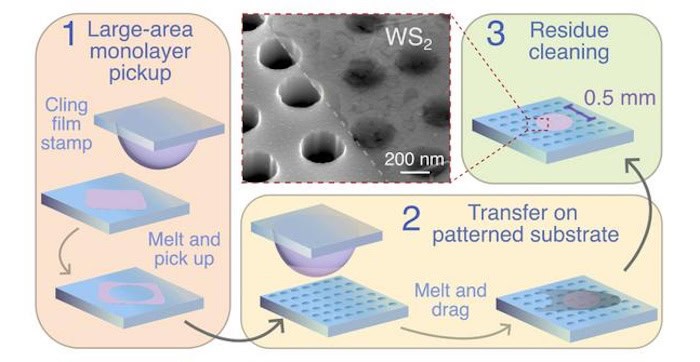
- The stamp contacts the layer at 70 C, is heated to 140 C so the polymer melts and grips it, then cooled back to 70 C to solidify before the layer is lifted away and cleaned of residue.
- The worked demonstration moved a gold-assisted-exfoliated tungsten disulphide monolayer from one silica substrate onto another silica substrate.
- The group also reports transferring hexagonal boron nitride heterostructures and TMDC monolayers onto substrates ranging from flat surfaces to high-aspect-ratio and low-adhesion patterned interfaces.
Compiled by The ScientistSomething wrong?How this is made
Why it matters
- capability Patterned substrates become legal targets, so a 2D layer can be placed onto contacts and optical coatings that already exist rather than having the device built around wherever the flake happened to land.
- constraint Anything already on the target has to survive the trip to 140 C and the residue clean, which quietly excludes stacks with temperature-sensitive layers or coatings that a solvent step would attack.
- cost The consumable costs pennies, so the real expense sits in the force-sensing micron-precision stage and the operator time each single placement occupies.
- precedent A yield claim published as a phrase rather than a ratio sets the bar the next group has to clear before anyone designs a fabrication flow assuming deterministic placement.
The switch is what deserves the attention here, not the shopping list. A conventional stamp transfer depends on a fixed adhesion contrast between stamp and target, and whether the layer stays behind is settled by contact history nobody can watch; van de Groep's word for those earlier methods, probabilistic, is the fair one [4]. Melting the polymer turns that contrast into a control knob. At 140 C the low-density polyethylene passes through a phase transition and grips the monolayer strongly, and cooling back to 70 C solidifies the grip before the stamp is pulled away [7]. The force sensors are there for the same reason: the approach halts at 120 mN of normal load, a setpoint the next operator can actually hit, and van de Groep says the in-plane channels also record friction dynamics through the contact [6][8].
Near-unity yield is the phrase to press on. It comes from the researcher who led the work, and the account carries no count of successes over attempts [4]. Near-unity over six placements and near-unity over six hundred are different claims, and only the second one is a process.
The other number worth holding is area. Gold-assisted exfoliation already delivers high-quality centimetre-sized TMDC layers onto flat glass [11]; this method places roughly a millimetre [3]. Ten times smaller on a side is a hundred times smaller in area, so one stamping cycle commits on the order of 1% of a centimetre-scale sheet [2]. For a nanophotonics test structure a square millimetre is room to spare. For anything wafer-scale it is a different problem sharing a name.
The method carries two constraints. The target has to tolerate the excursion to 140 C, a 70 C swing above the hold temperature, plus the clean that removes polymer residue afterwards [7][3]. That is a real filter precisely on the surfaces van de Groep says nanophotonics needs, the ones already carrying electrical contacts and optical coatings [14]. The stage also crawls: 0.5 micron per second works out to 30 microns per minute [1], one placement at a time under force feedback.
The researchers imaged the monolayer before and after the procedure, and Physics World reports that it retains its good photoluminescence properties [16]. What that does not tell you is how a device built this way behaves. An optical check on an intact sheet confirms photoluminescence and nothing more; it does not measure carrier mobility, contact resistance, or the crack count across a hundred transfers onto high-aspect-ratio topography, which is where a transfer method usually goes wrong in production rather than in a paper.
If the yield claim survives a denominator and an outside lab, what changes is the order of fabrication: the patterned device can be built first, and the 2D layer put where it belongs afterwards.
What to watch
- Whether the ACS Nano paper or a follow-up gives success-over-attempt counts, and whether an outside lab reproduces the yield on patterned topography.
- Whether transferred monolayers get electrical characterisation, such as mobility or contact resistance, rather than optical checks alone.
- Whether the placeable area grows from about a millimetre toward the centimetre sheets gold-assisted exfoliation already produces.