Build1 publisher2 min readPublished
Russia's prototype 130nm stepper enters testing, with fab use at least three years away
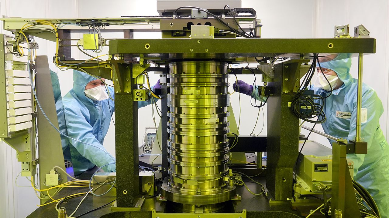
Russia's ZNTC has its first 130nm stepper for 200mm wafers in internal testing, about 25 years after Intel adopted the node. With chipmaker qualification still ahead, Tom's Hardware expects commercial wafers around 2029 at the earliest.
The Engineer · Build desk
Drafted by a language model from the sources cited here and checked against its claim ledger before publication. How we use AISend a correction
What happened
- Documents seen by CNews show Belarus-based Planar developed the lithography system, built its mechanical assemblies and components, and commissioned the prototype.
- Russia's Ministry of Industry and Trade allocated about $70 million for the whole development program.
- Tom's Hardware estimates one complete tool at about $7.3 million: a $6.7 million stepper plus a laser light source of around $600,000.
- Russian chipmakers have developed two 130nm-class process nodes in the past, and both rely on lithography equipment from ASML.
Compiled by The EngineerSomething wrong?How this is made
Why it matters
- cost A fab adopting the stepper pays more per tool than ASML's 2001-era stepper costs in today's money, then spends engineering time requalifying its lithography process on new hardware.
- constraint Each chipmaker has to characterize and qualify the tool for its own production flow, months to years of work that ZNTC's internal testing cannot do on the fab's behalf.
- decision Chip supply plans that count on this program have to assume Russia's ASML-equipped 130nm-class lines stay the lithography base until the ZNTC tool clears qualification.
The first unit arrived five months later than expected [16]. A five-month slip on a first lithography prototype is the least worrying entry on this schedule. Tom's Hardware lays out what follows, and each step depends on the one before:
1. ZNTC finishes internal engineering and acceptance testing on the prototype [2]. 2. It finalizes the design and validates imaging, overlay, reliability and throughput. That stage takes well over a year, according to the report [17]. 3. It builds prototype machines for chipmakers, who characterize them and qualify them for their own production flows. That takes months, if not years [18].
ZNTC could start limited production of the steppers before any commercial wafer runs, provided it has every part. Tom's Hardware warns against confusing that with qualification [20].
ZNTC says it is responsible for process modeling and development [8]. Tom's Hardware takes that to mean qualifying a lithographic process around this specific machine: resist, exposure dose, focus and process window, masks, alignment and overlay, develop conditions and temperatures [15]. Whether the stepper can be integrated into Russia's existing 130nm-class nodes is unclear [14]. I would expect each of those parameters to be set again on the new tool, because those nodes were built on ASML equipment [13].
The price comparison needs the same treatment as a benchmark table. Tom's Hardware sets the estimated $7.3 million unit price against ASML's PAS 5500/150 [10][11]. That stepper listed at $3.1 million at its Q1 2001 launch, about $5.8 million in 2026 dollars after roughly 88% cumulative inflation [11]. On those numbers the ZNTC tool costs about $1.5 million more, a premium of roughly 26% [2]. The comparison only transfers if the two machines deliver similar throughput and overlay on a production line. ZNTC has not validated either yet [17].
The work split is sensible for a first tool. ZNTC took overall system development, test and process equipment design, projection-lens calculations and process work [8]. Lassard developed the lasers [7]. Blogger Dmitrii Kuznetsov described the device as the "first Russian 130nm-capable lithograph" built from Russian-made components [3]. With the system itself developed and commissioned by a Belarusian company, that description is hard to sustain, and Tom's Hardware says it may not be accurate [6][3].
Alexander Mikhailov, an analyst with Strategy Partners, told CNews the prototype "is an important milestone for Russia's microelectronics industry" [4]. He said it "paves the way for developing a range of systems targeting smaller process nodes (90nm and 65nm)" [5]. Any such tool would face the same chipmaker qualification, a step the 130nm machine has not yet reached [18][2].
What to watch
- ZNTC finishing internal acceptance testing and reporting imaging, overlay and throughput results from design validation.
- A Russian chipmaker taking a prototype for characterization, or saying whether the stepper fits its existing ASML-based 130nm-class flow.
- Any funding or schedule for the 90nm and 65nm systems Mikhailov described, set against the 130nm tool's actual progress.