Science1 distinct publisher3 min readPublished
A Kyoto group's silicon carbide JFET holds its switching threshold at 600 C by putting the gate underneath the channel. The payoff sits in geothermal drilling and engine control as much as in any Venus lander.
The Scientist · Science desk

Compiled by The ScientistSomething wrong?How this is made
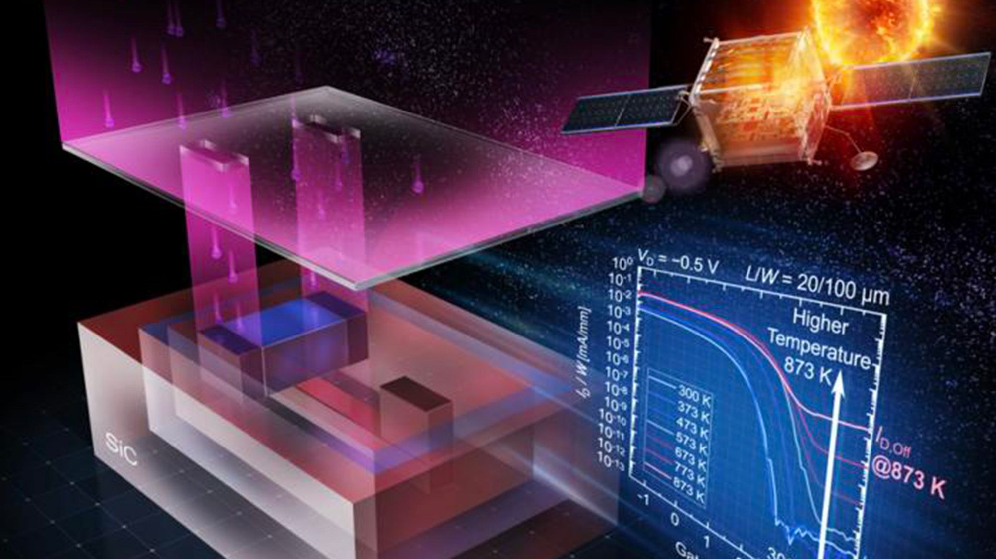
Start with the threshold voltage, because that is where the design work went. A JFET switches when the gate's field opens or pinches the channel, so where the switching point sits depends on exactly how much dopant sits where [2]. In silicon carbide, some dopant atoms travel deeper into the crystal than the process intended, and the Kyoto group reports that this can move a conventional JFET's threshold by more than 2 volts once the device is hot [12]. Their fix is geometric: put the gate beneath the channel and dope it heavily, so stray atoms arrive in a region already saturated with dopant and the channel-gate profile barely registers them [16]. Mitsuaki Kaneko, the study's first author, blames the field's slow progress on "trying to apply silicon-era thinking to a fundamentally different material" [15].
Leakage is the second of the two failures they set out to fix [11]. Above 350 C the substrate itself becomes less resistive, so current sneaks around the channel while the transistor is nominally off, producing wrong signals and unbudgeted power draw [13]. The answer was two doped wells around the device, whose boundaries block that bypass path even as the substrate turns conductive [17].
Worth putting the temperatures side by side. 600 C is 100 C above the 500 C at which the best previous JFETs could run long term [14][1], and 250 C above where the leakage problem starts [3]. Against Venus it leaves 140 C of margin over a surface that reaches 460 C [10][2]. But the limit the authors name for past missions is time, not peak heat: silicon electronics held landers to a few hours [8], and Venera 13's record on the surface is 2 hours 7 minutes, or 127 minutes [9][4]. What was measured here is how cleanly the device switches and how closely its threshold matched the value predicted from channel thickness and doping, across a range beginning at room temperature [18]. An operating lifetime at 600 C is not in that set.
On a lander, ambient temperature is not a design variable. In a turbine or a borehole it usually is, and the price is paid in cooling hardware and in the distance between a sensor and the electronics reading it, which is why geothermal drilling and aerospace engine control sit next to deep-space exploration in the authors' own list of targets [7]. The device family suits that work for a second reason: a JFET's operation does not depend on an oxide layer, which is where its lower noise comes from, and low noise is what a sensor front end wants [5]. The same physics caps its ambition, since JFETs are harder to shrink than the MOSFETs in consumer processors [4], so the integrated circuits this leads to will be modest ones by consumer standards. A switching point you can predict at temperature is the precondition for building any of them, and that, more than the 600 C label [1], is what the work demonstrates.
Ranked by verification strength, evidence, and original report placement.
Scientists in Japan built a new transistor that can withstand temperatures of 600 degrees Celsius (1,110 degrees Fahrenheit).
The researchers described the transistor in a study published Aug. 17 in the journal APL Electronic Devices.
Researchers measured how well the new JFET could switch current on and off and how closely the actual threshold voltage matched the theoretical value based on its thickness and level of doping, recording these metrics at temperatures ranging from room temperature upward.
The device is a junction field-effect transistor (JFET), in which the strength of an electrical field changes the channel's conductivity.
JFETs are typically used in specialist applications because they are harder to scale down than metal-oxide-semiconductor field-effect transistors (MOSFETs), which are widely used in consumer smartphones and computers.
JFETs can offer lower noise levels because their operation does not rely on an oxide layer, which can introduce interference.
Distinct publishers with included, body-backed reporting in this cluster.
1 article · September 6, 2026
Follow any of these and your For You feed starts watching them — no settings page required.
product
A five-watt nuclear heater on Blue Ghost turns lunar night into a procurement problem1 distinct publisher
science
ESA's Mercury orbiters cut themselves loose 200 million kilometres beyond real-time control3 distinct publishers
product
Swift will burn up, and LINK's consolation prize is the honest state of satellite servicing5 distinct publishers
science
NASA's two Sun papers ask paleoclimate to carry an astrophysical term2 distinct publishers
Evidence-backed comparisons of source perspectives and observed adoption signals. Read the methodology
Which Builder, Operator, and Investor concerns the observed source mix emphasized—not a truth score.
Evidence, demonstrated adoption, hype gap, incentives, and confidence are assessed independently, each on its own current evidence. How these are measured.
One paper, one outlet
The physics is specific and internally consistent: a named failure mode, a quantified error of more than 2 volts, a geometry that answers it, and a measured threshold error under 0.1 V at about 400 C. All of it reaches us through Live Science's reading of a single APL Electronic Devices paper plus a Kyoto statement, with no second measurement, no outside device engineer quoted, and no dimensions or circuit-level numbers to check the claim against.
Bench devices, no circuits yet
What exists is fabricated single transistors measured on a bench. The remaining steps are stated by the team: integration into complex circuits, scaling to wafer level, and a package that survives Venus-grade heat and pressure at once. The only field-scale datapoint in the story belongs to someone else, NASA's SiC-JFET circuits at 460 C and 9.3 MPa for 60 days, which shows the target is reachable without saying anything about this device.
Headline outruns the package
A Venus lander needs 460 C and about 9.3 MPa held for weeks, plus a whole circuit; what has been shown is a transistor that switches cleanly at 600 C. The headline's 'priming it for use in Venus-bound probes' does the recruiting, and Kyoto's own quote about silicon-era thinking is a claim about a community rather than a result. Live Science keeps the gap modest by printing the unfinished-work list and by noting the drilling and engine-control uses, which are the nearer targets.
Kyoto supplies the frame
The narrative arrives through a university statement: the diagnosis of why the field stalled, the quote that carries it, and the Venus framing that earns a device paper a general-audience headline. That is normal research communication rather than anything hidden, and Live Science's own interest in a striking number pulls the same direction. No commercial party appears in the story, which limits how far the incentive reaches.
Clear physics, thin corroboration
The device claims hang together and the numbers are precise enough to be tested by anyone with a probe station, so we are reasonably confident about what was measured. Confidence drops on everything past the bench: one outlet, one paper, an undated NASA comparison, and no manufacturing or commercial detail at all.