BuildNot yet confirmed elsewhere1 publisher3 min readPublished
LG sells an OSAT a 1.5-micron maskless imager, betting packaging capacity is the bottleneck
The tool tops out well short of DUV resolution. Its argument is throughput, 600 mm substrates and digital pattern correction while CoWoS supply stays tight.
The Engineer · Build desk
What happened
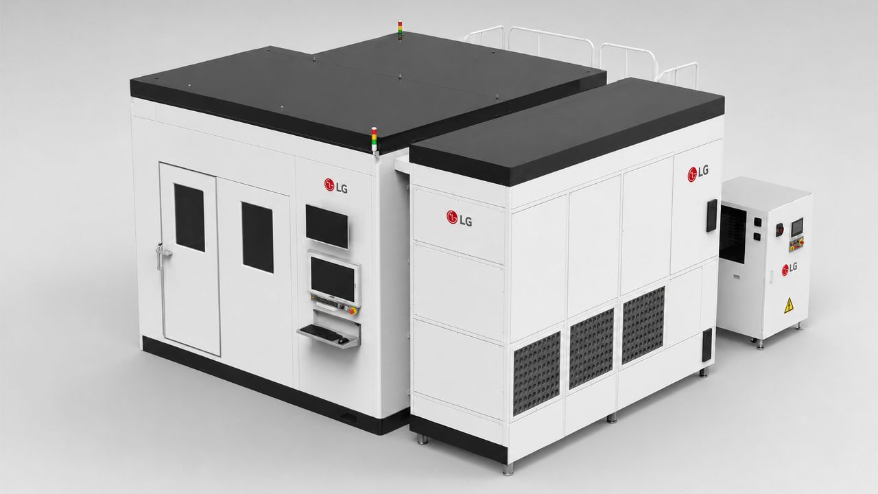
- This week, LG Electronics Production Technology Institute (PRI) signed a contract with an OSAT to supply a maskless laser direct imaging (LDI) lithography tool that can be used to build metal-interconnect patterns in semiconductor packaging, potentially with higher yields than currently available tools, reports ETNews.
- LDI in general cannot match the resolutions offered by modern DUV, EUV or e-beam lithography machines; it trades ultimate resolution for vastly higher throughput and large-area processing, suited to PCB and chip packaging production.
- TSMC's CoWoS advanced packaging capacity remains constrained.
- The LG production equipment uses a 405-nm laser-diode light source and can process substrates as large as 600 x 600 mm, according to various media reports.
- A 600 x 600 mm substrate is 0.36 square metres of exposure area.
Why it matters
LG Electronics' Production Technology Institute has signed a contract this week with an outsourced semiconductor assembly and test firm to supply a maskless laser direct imaging tool for patterning metal interconnects in chip packaging, with the vendor claiming potentially higher yields than currently available tools, according to ETNews as relayed by Tom's Hardware [1]. The interesting part is what the tool gives up: laser direct imaging cannot match modern DUV, EUV or e-beam resolution, and trades that for much higher throughput and large-area processing [3], which is a wager that the binding constraint in advanced packaging is capacity rather than linewidth, at a moment when TSMC's CoWoS remains constrained [17].
The hardware, per various media reports cited by Tom's Hardware, uses a 405-nm laser-diode source and handles substrates up to 600 x 600 mm [4]. That is 0.36 square metres of substrate per plate [15]. The highest-resolution version of the system prints 1.5-micron line-and-space patterns, good for wiring pitches of roughly 3 microns [5].
Where that number lands is the whole story. TSMC's CoWoS-R and CoWoS-L use RDL interposers with a minimum 4-micron pitch, or 2-micron line width and spacing [6], so 1.5 microns leaves about half a micron of headroom against that layer [16]. It does not go further. Both CoWoS-S and CoWoS-L/EMIB-like schemes require considerably higher resolution than current-generation LDI, which makes the RDL interposer the most advanced structure these machines can pattern [7]. LG is selling into the substrate and redistribution-layer tier, not into the interposer tier that defines the packaging roadmap.
It is also not walking into an empty room. The direct-imaging market is led by KLA, Screen Holdings, Limata and ORC, with roughly a dozen participants from Germany, France, Switzerland, Japan and China [8], and competing products already ship in 1-micron, 3-micron and 5-micron variants [9]. LG's 1.5-micron figure targets the higher end without being the finest thing on the market, and the plan is to price competitively [18].
The more durable technical argument is not resolution at all. Because the pattern is generated digitally by a pattern generator and projection optics rather than transferred through a photomask, the system can create and calibrate patterns in real time [10]. That matters because packaging substrate geometry varies and organic substrates expand, contract or warp during processing [11]. At 1.5-micron wiring, a shift from the nominal layout can produce a solder bridge or a faulty contact, which is yield loss [12]. Mask-based flows cannot chase a warped panel; a digital one can.
Context on the seller: unlike Samsung and SK Group, LG Group does not produce chips, though its divisions supply materials and components to the industry [13]. The system is positioned for advanced packaging on organic and later glass substrates, plus displays, MEMS, and high-density or prototype PCBs [14].
What to watch. The buyer is not identified in the report [2], so the volume and the application tier are unknown. Watch whether the stated glass-substrate path arrives with the resolution intact, since glass removes the warpage problem that justifies digital correction in the first place [11][14]. And watch pricing: against incumbents with 1-micron tools already in the field [9], competitive pricing [18] is the only lever LG has named.
Clarity's read
What the record supports and how the coverage leans. The claims behind it follow.
Reality
- Evidence42
- Adoption22
- Hype gap+18
- Incentives58
- Confidence45
Claim ledger
Ranked by verification strength, evidence, and original report placement.
- [1]
This week, LG Electronics Production Technology Institute (PRI) signed a contract with an OSAT to supply a maskless laser direct imaging (LDI) lithography tool that can be used to build metal-interconnect patterns in semiconductor packaging, potentially with higher yields than currently available tools, reports ETNews.
ReportedSupportedSource: ETNews, via Tom's Hardware2 sources— create a free account to open themView cited source - [2]
The report does not identify the OSAT that signed the supply contract with LG-PRI.
- [3]
LDI in general cannot match the resolutions offered by modern DUV, EUV or e-beam lithography machines; it trades ultimate resolution for vastly higher throughput and large-area processing, suited to PCB and chip packaging production.
- [4]
The LG production equipment uses a 405-nm laser-diode light source and can process substrates as large as 600 x 600 mm, according to various media reports.
- [5]
LG has developed various versions of the machine; its highest-resolution version can produce 1.5-micron line-and-space patterns, which should be fine enough to print wiring pitches of about 3 microns.
- [6]
TSMC CoWoS-R and CoWoS-L use RDL interposers with a minimum 4-micron pitch, or 2-micron line width/spacing.
- [7]
With current-generation LDI, the RDL interposer is the most advanced structure these devices can pattern, as both CoWoS-S and CoWoS-L/EMIB-like technologies require considerably higher resolution.
- [8]
The direct-imaging market is already established and led by KLA, Screen Holdings, Limata and ORC, with about a dozen manufacturers participating from Germany, France, Switzerland, Japan and China.
- [9]
Competing direct-imaging products offer 1-micron, 3-micron and 5-micron versions for different applications.
- [10]
In LDI the pattern is generated digitally by a digitally controlled pattern generator and projection optics instead of a photomask, so the system can create and calibrate patterns in real time, with projection optics, precision alignment and stage control positioning the pattern on the substrate.
- [11]
Real-time pattern adjustment matters because the dimensions and geometry of packaging substrates can vary and because organic substrates can expand, contract or warp during processing.
- [12]
At 1.5-micron-scale wiring, any shift from the nominal layout may result in a solder bridge or a faulty contact, which means yield loss.
- [13]
Unlike Samsung and SK Group, LG Group does not produce chips, although its divisions supply various materials and components for the semiconductor industry.
- [14]
LG positions its LDI system primarily for advanced semiconductor packaging using organic and then glass substrates, displays and MEMS, and it can also build high-density PCBs for mobile devices or prototyping.
- [15]
A 600 x 600 mm substrate is 0.36 square metres of exposure area.
- [16]
LG's 1.5-micron line/space capability is about 0.5 microns finer than the 2-micron line width/spacing cited for CoWoS-R/-L RDL interposers.
- [17]
TSMC's CoWoS advanced packaging capacity remains constrained.
ReportedInsufficientSource: Tom's Hardware2 sources— create a free account to open themView cited source - [18]
LG's 1.5-micron line/space capability targets the higher end of the market, and to establish a position LG plans to price its LDI system competitively.
Sources
1 independent publisher whose own reporting we read for this story.
Topics and entities
Follow any of these and your For You feed starts watching them — no settings page required.