Loading today’s stories
Science1 distinct publisher3 min readUpdated
AI-drawn photonic parts land 500x smaller, and that is a die-area story
Three inverse-designed components were fabricated and measured in a May 28 Nature Communications paper. The shrink is real; the integrated circuit does not exist yet.
The Scientist · Science desk
What happened
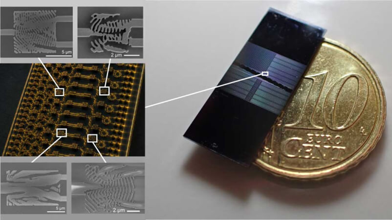
- Scientists shrank three components used in photonic microchips by up to 500 times, leaving considerably more space for other on-chip functionality, using an AI algorithm that generated the designs.
- The researchers described the AI-generated designs as "beyond human intuition."
- The researchers published their findings on May 28 in the journal Nature Communications.
- The three components fabricated on an ultracompact scale were wavelength splitters, spatial mode sorters and mirrors, all essential for separating and directing different wavelengths and light patterns.
- Instead of metal wires, micrometer-wide channels called waveguides direct light across a photonic chip.
Compiled by The ScientistSomething wrong?How this is made
Why it matters
An inverse-design algorithm produced three photonic chip components up to 500 times smaller than the hand-engineered versions they replace, and the researchers fabricated them and published the measurements on May 28 in Nature Communications [1][3]. The interesting number is not the shrink factor but what it does to a die: at 500x, a part occupies roughly 0.2 percent of its former footprint [1], and the authors argue the freed space lets engineers pack in more components and "unlock new functionalities" [14].
The three parts are a wavelength splitter, a spatial mode sorter, and mirrors, the plumbing that separates and steers different wavelengths and light patterns on a chip where micrometer-wide waveguides do the job metal wires do in electronics [4][5]. The splitter is about 5 micrometers across, roughly the size of a single bacterium, and the mode sorter is marginally larger [13]. The mirrors are about 11 micrometers long and reflect up to 98.5 percent of incoming light while blocking unwanted light patterns [11]; placed in pairs on either side of a waveguide, light bounced between them more than 100 times before escaping [12]. The two figures hang together: 98.5 percent per reflection compounds to about 22 percent survival across 100 bounces [2].
The method matters more than any single part. The team told the algorithm what it wanted light to do and supplied fabrication constraints, including limits on how sharply the nanostructures could curve, then let it work backward, testing and refining designs until it found structures that met the specification [6]. "Inverse design lets us define what we want light to do, and the optimization finds a structure that does it, often one no human would have drawn," said study first author Toby Bi, a researcher at the Max Planck Institute for the Science of Light [7]. Bi also said the same framework handled three different jobs on one chip: routing light by wavelength, sorting it by spatial mode, and acting as compact mirrors that form on-chip optical cavities [8]. Standard practice is the opposite: engineers begin from a proven geometry and optimize it by hand for each new performance target, which is slow and limits the range of device geometries anyone ever tries [9].
The material choice is part of the result. The components were built in relatively thick silicon nitride, roughly 400 to 800 nanometers, against 150 to 400 nanometers for standard silicon, which wastes less light and confines wavelengths more strongly [10]. At the thin end that nitride only matches the thickest standard silicon layer; at the thick end it is more than five times the thinnest [3].
Integration is what to watch. The components have been demonstrated individually and have not been combined into a complete integrated optical circuit, which the researchers call the next step toward chips that actually use the added density [15]. Until that part lands, the 500x is a per-component claim rather than a chip-level one. Demand is not the constraint: photonic chips already ship into fiber-optic communications, data centers, AI, automotive lidar and quantum computing [16], where separate wavelengths carry distinct data streams and less energy is lost as heat [17]. The open question for anyone specifying a photonic process is whether curvature-constrained, machine-drawn geometries hold their yield when dozens of them sit side by side on the same die.
Topics and entities
Follow any of these and your For You feed starts watching them — no settings page required.
Topics
Loading related stories